SNVSB96 July 2019 LM3424-Q1
PRODUCTION DATA.
- 1 Features
- 2 Applications
- 3 Description
- 4 Revision History
- 5 Pin Configuration and Functions
- 6 Specifications
-
7 Detailed Description
- 7.1 Overview
- 7.2 Functional Block Diagram
- 7.3
Feature Description
- 7.3.1 Current Regulators
- 7.3.2 Peak Current Mode Control
- 7.3.3 Average LED Current
- 7.3.4 Thermal Foldback and Analog Dimming
- 7.3.5 Current Sense and Current Limit
- 7.3.6 Slope Compensation
- 7.3.7 Control Loop Compensation
- 7.3.8 Start-Up Regulator and Soft-Start
- 7.3.9 Overvoltage Lockout (OVLO)
- 7.3.10 Input Undervoltage Lockout (UVLO)
- 7.3.11 PWM Dimming
- 7.3.12 Thermal Shutdown
- 7.4 Device Functional Modes
-
8 Application and Implementation
- 8.1 Application Information
- 8.2
Typical Applications
- 8.2.1
Basic Topology Schematics
- 8.2.1.1 Design Requirements
- 8.2.1.2
Detailed Design Procedure
- 8.2.1.2.1 Operating Point
- 8.2.1.2.2 Switching Frequency
- 8.2.1.2.3 Average LED Current
- 8.2.1.2.4 Thermal Foldback
- 8.2.1.2.5 Inductor Ripple Current
- 8.2.1.2.6 LED Ripple Current
- 8.2.1.2.7 Peak Current Limit
- 8.2.1.2.8 Slope Compensation
- 8.2.1.2.9 Loop Compensation
- 8.2.1.2.10 Input Capacitance
- 8.2.1.2.11 NFET
- 8.2.1.2.12 Diode
- 8.2.1.2.13 Output OVLO
- 8.2.1.2.14 Input UVLO
- 8.2.1.2.15 Soft-Start
- 8.2.1.2.16 PWM Dimming Method
- 8.2.1.2.17 Analog Dimming Method
- 8.2.2
Buck-Boost Application
- 8.2.2.1 Design Requirements
- 8.2.2.2
Detailed Design Procedure
- 8.2.2.2.1 Operating Point
- 8.2.2.2.2 Switching Frequency
- 8.2.2.2.3 Average LED Current
- 8.2.2.2.4 Thermal Foldback
- 8.2.2.2.5 Inductor Ripple Current
- 8.2.2.2.6 Output Capacitance
- 8.2.2.2.7 Peak Current Limit
- 8.2.2.2.8 Slope Compensation
- 8.2.2.2.9 Loop Compensation
- 8.2.2.2.10 Input Capacitance
- 8.2.2.2.11 NFET
- 8.2.2.2.12 Diode
- 8.2.2.2.13 Input UVLO
- 8.2.2.2.14 Output OVLO
- 8.2.2.2.15 Soft-Start
- 8.2.2.3 Application Curve
- 8.2.3 Boost Application
- 8.2.4 Buck-Boost Application
- 8.2.5 Boost Application
- 8.2.6 Buck-Boost Application
- 8.2.7 Buck Application
- 8.2.8 Buck-Boost Application
- 8.2.9 SEPIC Application
- 8.2.1
Basic Topology Schematics
- 9 Power Supply Recommendations
- 10Layout
- 11Device and Documentation Support
- 12Mechanical, Packaging, and Orderable Information
7.3.11 PWM Dimming
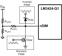
The active low nDIM pin can be driven with a PWM signal which controls the main NFET and the dimming FET (dimFET). The brightness of the LEDs can be varied by modulating the duty cycle of this signal. LED brightness is approximately proportional to the PWM signal duty cycle, (that is, 30% duty cycle at approximately 30% LED brightness). This function can be ignored if PWM dimming is not required by using nDIM solely as a VIN UVLO input as described in the Input Undervoltage Lockout (UVLO) section or by tying it directly to VCC or VIN.
 Figure 31. PWM Dimming Circuit
 Figure 31 shows how the PWM signal is applied to nDIM:
- Connect the dimming MOSFET (QDIM) with the drain to the nDIM pin and the source to GND. Apply an external logic-level PWM signal to the gate of QDIM.
- Connect the anode of a Schottky diode (DDIM) to the nDIM pin. Apply an inverted external logic-level PWM signal to the cathode of the same diode.
The DDRV pin is a PWM output that follows the nDIM PWM input signal. When the nDIM pin rises, the DDRV pin rises and the PWM latch reset signal is removed allowing the main MOSFET Q1 to turn on at the beginning of the next clock set pulse. In boost and buck-boost topologies, the DDRV pin is used to control a N-channel MOSFET placed in series with the LED load, while it would control a P-channel MOSFET in parallel with the load for a buck topology.
The series dimFET will open the LED load, when nDIM is low, effectively speeding up the rise and fall times of the LED current. Without any dimFET, the rise and fall times are limited by the inductor slew rate and dimming frequencies above 1 kHz are impractical. Using the series dimFET, dimming frequencies up to 30 kHz are achievable. With a parallel dimFET (buck topology), even higher dimming frequencies are achievable.
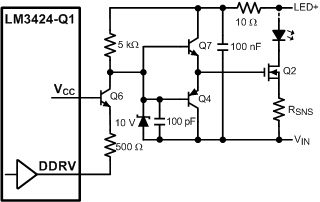
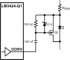
When using the PWM functionality in a boost regulator, the PWM signal drives a ground referenced FET. However, with buck-boost and buck topologies, level shifting circuitry is necessary to translate the PWM dim signal to the floating dimFET as shown in Figure 32 and Figure 33.
When using a series dimFET to PWM dim the LED current, more output capacitance is always better. A general rule of thumb is to use a minimum of 40 µF when PWM dimming. For most applications, this will provide adequate energy storage at the output when the dimFET turns off and opens the LED load. Then when the dimFET is turned back on, the capacitance helps source current into the load, improving the LED current rise time.
A minimum on-time must be maintained in order for PWM dimming to operate in the linear region of its transfer function. Because the controller is disabled during dimming, the PWM pulse must be long enough such that the energy intercepted from the input is greater than or equal to the energy being put into the LEDs. For boost and buck-boost regulators, the minimum dimming pulse length in seconds (tPULSE) is:

Even maintaining a dimming pulse greater than tPULSE, preserving linearity at low dimming duty cycles is difficult. Several modifications are suggested for applications requiring low dimming duty cycles. Since nDIM rising releases the latch but does not trigger the on-time specifically, there will be an effective jitter on the rising edge of the LED current. This jitter can be easily removed by tying the PWM input signal through the synchronization network at the RT pin (shown in ), forcing the on-time to synchronize with the nDIM pulse.
The second helpful modification is to remove the CFS capacitor and RFS resistor, eliminating the high frequency compensation pole. This should not affect stability, but it will speed up the response of the CSH pin, specifically at the rising edge of the LED current when PWM dimming, thus improving the achievable linearity at low dimming duty cycles.
 Figure 32. Buck-Boost Level-Shifted PWM Circuit
  Figure 33. Buck Level-Shifted PWM Circuit