SNVS616H April 2009 – July 2015 LM3429 , LM3429-Q1
PRODUCTION DATA.
- 1 Features
- 2 Applications
- 3 Description
- 4 Revision History
- 5 Pin Configuration and Functions
- 6 Specifications
-
7 Detailed Description
- 7.1 Overview
- 7.2 Functional Block Diagram
- 7.3
Feature Description
- 7.3.1 Current Regulators
- 7.3.2 Predictive Off-Time (PRO) Control
- 7.3.3 Switching Frequency
- 7.3.4 Average LED Current
- 7.3.5 Analog Dimming
- 7.3.6 Current Sense and Current Limit
- 7.3.7 Control Loop Compensation
- 7.3.8 Output Overvoltage Lockout (OVLO)
- 7.3.9 Input Undervoltage Lockout (UVLO)
- 7.3.10 PWM Dimming
- 7.3.11 Startup Regulator (VCC LDO)
- 7.3.12 Thermal Shutdown
- 7.4 Device Functional Modes
-
8 Application and Implementation
- 8.1 Application Information
- 8.2
Typical Applications
- 8.2.1
Basic Topology Schematics
- 8.2.1.1 Design Requirements
- 8.2.1.2
Detailed Design Procedure
- 8.2.1.2.1 Operating Point
- 8.2.1.2.2 Switching Frequency
- 8.2.1.2.3 Average LED Current
- 8.2.1.2.4 Inductor Ripple Current
- 8.2.1.2.5 LED Ripple Current
- 8.2.1.2.6 Peak Current Limit
- 8.2.1.2.7 Loop Compensation
- 8.2.1.2.8 Input Capacitance
- 8.2.1.2.9 NFET
- 8.2.1.2.10 Diode
- 8.2.1.2.11 Output OVLO
- 8.2.1.2.12 Input UVLO
- 8.2.1.2.13 PWM Dimming Method
- 8.2.1.2.14 Analog Dimming Method
- 8.2.2
Buck-Boost Application - 6 LEDs at 1 A
- 8.2.2.1 Design Requirements
- 8.2.2.2
Detailed Design Procedure
- 8.2.2.2.1 Operating Point
- 8.2.2.2.2 Switching Frequency
- 8.2.2.2.3 Average LED Current
- 8.2.2.2.4 Inductor Ripple Current
- 8.2.2.2.5 Output Capacitance
- 8.2.2.2.6 Peak Current Limit
- 8.2.2.2.7 Loop Compensation
- 8.2.2.2.8 Input Capacitance
- 8.2.2.2.9 NFET
- 8.2.2.2.10 Diode
- 8.2.2.2.11 Input UVLO
- 8.2.2.2.12 Output OVLO
- 8.2.2.3 Application Curve
- 8.2.3 Boost PWM Dimming Application - 9 LEDs at 1 A
- 8.2.4 Buck-Boost Analog Dimming Application - 4 LEDs at 2A
- 8.2.5 Boost Analog Dimming Application - 12 LEDs at 700 mA
- 8.2.6 Buck-Boost PWM Dimming Application - 6 LEDs at 500 mA
- 8.2.7 Buck Application - 3 LEDS at 1.25 A
- 8.2.8 Buck-Boost Thermal Foldback Application - 8 LEDs at 2.5 A
- 8.2.9 SEPIC Application - 5 LEDs at 750 mA
- 8.2.1
Basic Topology Schematics
- 9 Power Supply Recommendations
- 10Layout
- 11Device and Documentation Support
- 12Mechanical, Packaging, and Orderable Information
6 Specifications
6.1 Absolute Maximum Ratings
over operating free-air temperature range (unless otherwise noted)(1)(2)| MIN | MAX | UNIT | ||
|---|---|---|---|---|
| Voltage | VIN, nDIM | –0.3 | 76 | V |
| OVP, HSP, HSN | –0.3 | 76 | ||
| RCT | –0.3 | 3 | ||
| IS | –0.3 | 76 | ||
| –2 for 100 ns | ||||
| VCC | –0.3 | 8 | ||
| COMP, CSH | –0.3 | 6 | ||
| GATE | –0.3 | VCC | ||
| –2.5 for 100 ns | VCC+2.5 for 100 ns | |||
| PGND | –0.3 | 0.3 | ||
| –2.5 | 2.5 for 100 ns | |||
| Continuous Current | VIN, nDIM | –1 | mA | |
| OVP, HSP, HSN | –100 | µA | ||
| RCT | –1 | 5 | mA | |
| IS | –1 | |||
| COMP, CSH | –200 | 200 | µA | |
| GATE | –1 | 1 | mA | |
| Maximum Junction Temperature | Internally Limited | |||
| Maximum Lead Temperature (Reflow and Solder) (3) | 260 | °C | ||
| Continuous Power Dissipation | Internally Limited | |||
| Storage Temperature, Tstg | –65 | 150 | °C | |
(1) Stresses beyond those listed under Absolute Maximum Ratings may cause permanent damage to the device. These are stress ratings only, which do not imply functional operation of the device at these or any other conditions beyond those indicated under Recommended Operating Conditions. Exposure to absolute-maximum-rated conditions for extended periods may affect device reliability.
(2) If Military/Aerospace specified devices are required, contact the Texas Instruments Sales Office/Distributors for availability and specifications.
(3) Refer to http://www.ti.com/packaging for more detailed information and mounting techniques.
6.2 ESD Ratings
| VALUE | UNIT | ||||
|---|---|---|---|---|---|
| LM3429 IN PWP PACKAGE | |||||
| V(ESD) | Electrostatic discharge | Human body model (HBM), per ANSI/ESDA/JEDEC JS-001, all pins(1) | ±2000 | V | |
| Charged device model (CDM), per JEDEC specification JESD22-C101, all pins(2) | ±1000 | ||||
| LM3429-Q1 IN PWP PACKAGE | |||||
| V(ESD) | Electrostatic discharge | Human body model (HBM), per AEC Q100-002(3) | ±2000 | V | |
| Charged device model (CDM), per AEC Q100-011 | ±1000 | ||||
(1) JEDEC document JEP155 states that 500-V HBM allows safe manufacturing with a standard ESD control process.
(2) JEDEC document JEP157 states that 250-V CDM allows safe manufacturing with a standard ESD control process.
(3) AEC Q100-002 indicates HBM stressing is done in accordance with the ANSI/ESDA/JEDEC JS-001 specification.
6.3 Recommended Operating Conditions
| MIN | MAX | UNIT | |
|---|---|---|---|
| Operating Junction Temperature Range | –40 | 125 | °C |
| Input Voltage VIN | 4.5 | 75 | V |
6.4 Thermal Information
| THERMAL METRIC(1) | LM3429-Q1 | LM3429 | UNIT | |
|---|---|---|---|---|
| PWP (HTSSOP) | PWP (HTSSOP) | |||
| 14 PINS | 14 PINS | |||
| RθJA | Junction-to-ambient thermal resistance | 47.8 | 47.8 | °C/W |
| RθJC(top) | Junction-to-case (top) thermal resistance | 26.5 | 26.5 | °C/W |
| RθJB | Junction-to-board thermal resistance | 22.3 | 22.3 | °C/W |
| ψJT | Junction-to-top characterization parameter | 0.7 | 0.7 | °C/W |
| ψJB | Junction-to-board characterization parameter | 22.1 | 22.1 | °C/W |
| RθJC(bot) | Junction-to-case (bottom) thermal resistance | 3.3 | 3.3 | °C/W |
(1) For more information about traditional and new thermal metrics, see the Semiconductor and IC Package Thermal Metrics application report, SPRA953.
6.5 Electrical Characteristics
MIN and MAX limits apply TJ = (−40°C to 125°C) unless specified otherwise. Unless otherwise stated the following condition applies: VIN = 14 V.| PARAMETER | TEST CONDITIONS | MIN(1) | TYP(2) | MAX(1) | UNIT | |
|---|---|---|---|---|---|---|
| STARTUP REGULATOR (VCC) | ||||||
| VCC-REG | VCC Regulation | ICC = 0 mA | 6.3 | 6.9 | 7.35 | V |
| ICC-LIM | VCC Current Limit | VCC = 0V | 20 | 27 | mA | |
| IQ | Quiescent Current | Static | 1.6 | 3 | ||
| VCC-UVLO | VCC UVLO Threshold | VCC Increasing | 4.17 | 4.5 | V | |
| VCC Decreasing | 3.7 | 4.08 | ||||
| VCC-HYS | VCC UVLO Hysteresis | 0.1 | ||||
| OVERVOLTAGE PROTECTION (OVP) | ||||||
| VTH-OVP | OVP OVLO Threshold | OVP Increasing | 1.18 | 1.24 | 1.28 | V |
| IHYS-OVP | OVP Hysteresis Source Current | OVP Active (high) | 10 | 20 | 30 | µA |
| ERROR AMPLIFIER | ||||||
| VCSH | CSH Reference Voltage | With Respect to AGND | 1.21 | 1.235 | 1.26 | V |
| Error Amplifier Input Bias Current | MIN, MAX: TJ = 25°C | –0.6 | 0 | 0.6 | µA | |
| COMP Sink / Source Current | 10 | 26 | 40 | |||
| Transconductance | 100 | µA/V | ||||
| Linear Input Range | (3) | ±125 | mV | |||
| Transconductance Bandwidth | -6dB Unloaded Response(3), MIN: TJ = 25°C | 0.5 | 1 | MHz | ||
| OFF TIMER (RCT) | ||||||
| tOFF-MIN | Minimum Off-time | RCT = 1V through 1 kΩ | 35 | 75 | ns | |
| RRCT | RCT Reset Pulldown Resistance | 36 | 120 | Ω | ||
| VRCT | VIN/25 Reference Voltage | VIN = 14V | 540 | 565 | 585 | mV |
| PWM COMPARATOR | ||||||
| COMP to PWM Offset | 700 | 800 | 900 | mV | ||
| CURRENT LIMIT (IS) | ||||||
| VLIM | Current Limit Threshold | 215 | 245 | 275 | mV | |
| VLIM Delay to Output | 35 | 75 | ns | |||
| tON-MIN | Leading Edge Blanking Time | 75 | 250 | 450 | ||
| HIGH SIDE TRANSCONDUCTANCE AMPLIFIER | ||||||
| Input Bias Current | 10 | µA | ||||
| Transconductance | 20 | 119 | mA/V | |||
| Input Offset Current | –1.5 | 0 | 1.5 | µA | ||
| Input Offset Voltage | –7 | 0 | 7 | mV | ||
| Transconductance Bandwidth | ICSH = 100 µA(3), MIN: TJ = 25°C | 250 | 500 | kHz | ||
| GATE DRIVER (GATE) | ||||||
| RSRC(GATE) | GATE Sourcing Resistance | GATE = High | 2 | 6 | Ω | |
| RSNK(GATE) | GATE Sinking Resistance | GATE = Low | 1.3 | 4.5 | ||
| UNDERVOLTAGE LOCKOUT and DIM INPUT (nDIM) | ||||||
| VTH-nDIM | nDIM / UVLO Threshold | 1.18 | 1.24 | 1.28 | V | |
| IHYS-nDIM | nDIM Hysteresis Current | 10 | 20 | 30 | µA | |
| THERMAL SHUTDOWN | ||||||
| TSD | Thermal Shutdown Threshold | (3) | 165 | °C | ||
| THYS | Thermal Shutdown Hysteresis | (3) | 25 | |||
(1) All limits specified at room temperature (TYP) and at temperature extremes (MIN/MAX). All room temperature limits are 100% production tested. All limits at temperature extremes are specified through correlation using standard Statistical Quality Control (SQC) methods. All limits are used to calculate Average Outgoing Quality Level (AOQL).
(2) Typical numbers are at 25°C and represent the most likely norm.
(3) These electrical parameters are specified by design, and are not verified by test.
6.6 Typical Characteristics
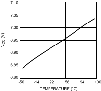
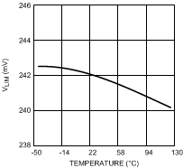
TA= 25°C and VIN = 14 V unless otherwise specified. The measurements for Figure 1 and Figure 3 were made using the standard boost evaluation board from AN-1986 (SNVA404). The measurements for Figure 2, Figure 4, and Figure 5, Figure 6 were made using the standard buck-boost evaluation board from AN-1985 (SNVA403).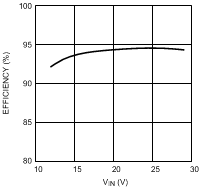
VO = 32 V (9 LEDs)
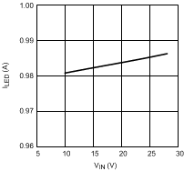
VO = 32 V (9 LEDs)
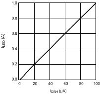
VO = 20 V (6 LEDs)
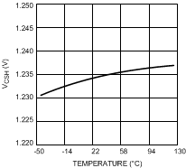
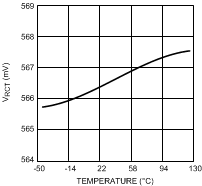
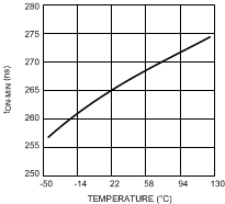
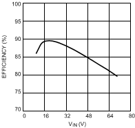
VO = 20 V (6 LEDs)
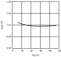
VO = 20 V (6 LEDs)
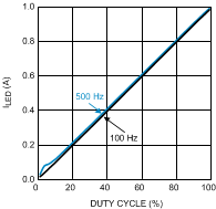
VO = 20V (6 LEDs)
