SNVS085X July 2000 – December 2017 LM3478
PRODUCTION DATA.
- 1 Features
- 2 Applications
- 3 Description
- 4 Revision History
- 5 Pin Configuration and Functions
- 6 Specifications
- 7 Detailed Description
-
8 Application and Implementation
- 8.1 Application Information
- 8.2
Typical Applications
- 8.2.1
Typical High Efficiency Step-Up (Boost) Converter
- 8.2.1.1 Design Requirements
- 8.2.1.2
Detailed Design Procedure
- 8.2.1.2.1 Custom Design with WEBENCH Tools
- 8.2.1.2.2 Power Inductor Selection
- 8.2.1.2.3 Programming the Output Voltage
- 8.2.1.2.4 Setting the Current Limit
- 8.2.1.2.5 Current Limit with External Slope Compensation
- 8.2.1.2.6 Power Diode Selection
- 8.2.1.2.7 Power MOSFET Selection
- 8.2.1.2.8 Input Capacitor Selection
- 8.2.1.2.9 Output Capacitor Selection
- 8.2.1.2.10 Compensation
- 8.2.1.3 Application Curves
- 8.2.2 Typical SEPIC Converter
- 8.2.1
Typical High Efficiency Step-Up (Boost) Converter
- 9 Power Supply Recommendations
- 10Layout
- 11Device and Documentation Support
- 12Mechanical, Packaging, and Orderable Information
7.3.2 Slope Compensation Ramp
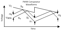
The LM3478 uses a current mode control scheme. The main advantages of current mode control are inherent cycle-by-cycle current limit for the switch and simpler control loop characteristics. It is also easy to parallel power stages using current mode control since current sharing is automatic. However, current mode control has an inherent instability for duty cycles greater than 50%, as shown in Figure 22.
A small increase in the load current causes the switch current to increase by ΔI0. The effect of this load change is ΔI1.
The two solid waveforms shown are the waveforms compared at the internal pulse width modulator, used to generate the MOSFET drive signal. The top waveform with the slope Se is the internally generated control waveform VC. The bottom waveform with slopes Sn and Sf is the sensed inductor current waveform VSEN.
 Figure 22. Sub-Harmonic Oscillation for D>0.5 and Compensation Ramp to Avoid Sub-Harmonic Oscillation
Sub-harmonic Oscillation can be easily understood as a geometric problem. If the control signal does not have slope, the slope representing the inductor current ramps up until the control signal is reached and then slopes down again. If the duty cycle is above 50%, any perturbation will not converge but diverge from cycle to cycle and causes sub-harmonic oscillation.
It is apparent that the difference in the inductor current from one cycle to the next is a function of Sn, Sf and Se as shown in Equation 1.

Hence, if the quantity (Sf - Se)/(Sn + Se) is greater than 1, the inductor current diverges and sub-harmonic oscillation results. This counts for all current mode topologies. The LM3478 has some internal slope compensation VSL which is enough for many applications above 50% duty cycle to avoid sub-harmonic oscillation .
For boost applications, the slopes Se, Sf and Sn can be calculated with Equation 2, Equation 3, and Equation 4.
When Se increases, then the factor that determines if sub-harmonic oscillation will occur decreases. When the duty cycle is greater than 50%, and the inductance becomes less, the factor increases.
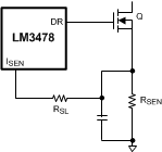
For more flexibility, slope compensation can be increased by adding one external resistor, RSL, in the ISEN's path. Figure 23 shows the setup. The externally generated slope compensation is then added to the internal slope compensation of the LM3478. When using external slope compensation, the formula for Se becomes:
A typical value for factor K is 40 µA.
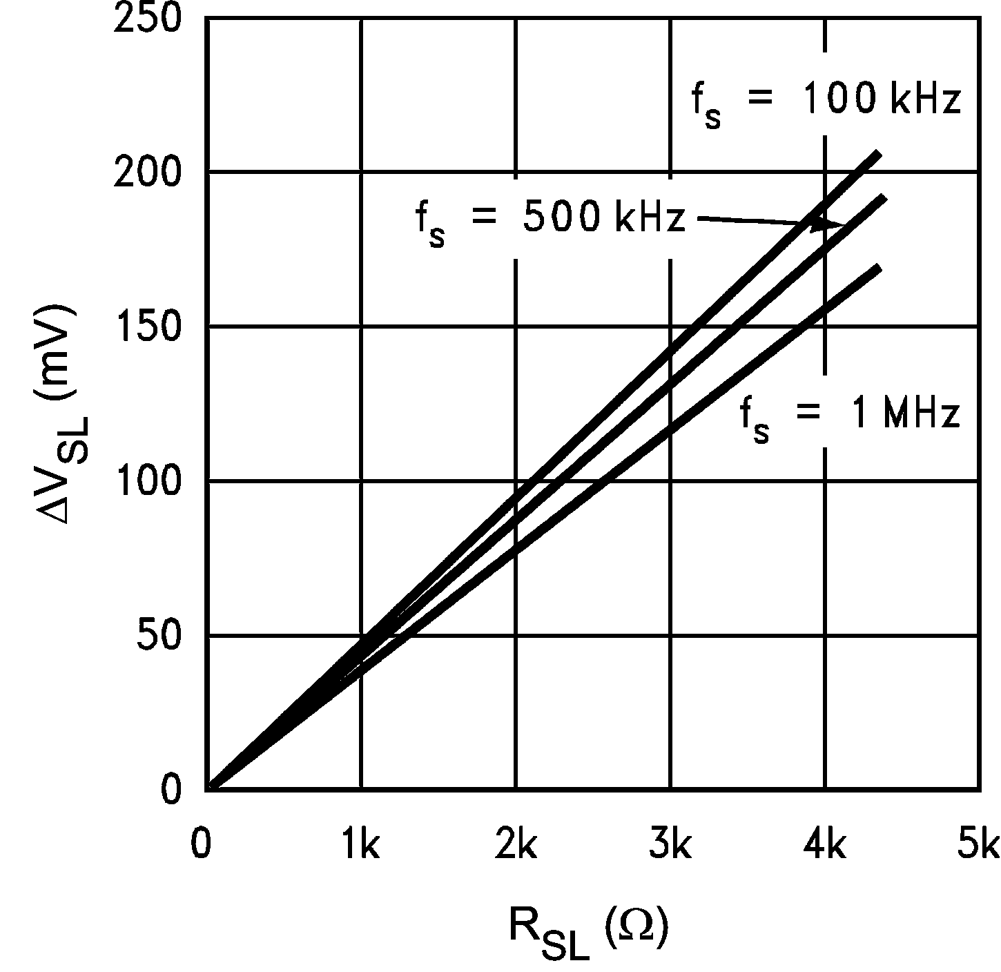
The factor changes with switching frequency. Figure 24 is used to determine the factor K for individual applications and Equation 6 gives the factor K.
It is a good design practice to only add as much slope compensation as needed to avoid sub-harmonic oscillation. Additional slope compensation minimizes the influence of the sensed current in the control loop. With very large slope compensation the control loop characteristics are similar to a voltage mode regulator which compares the error voltage to a saw tooth waveform rather than the inductor current.


ΔVSL vs RSL