ZHCSI45 April   2018 LM3478Q-Q1

PRODUCTION DATA.  

  1. 特性
  2. 应用
  3. 说明
    1.     Device Images
      1.      典型的高效升压转换器
  4. 修订历史记录
  5. Pin Configuration and Functions
    1.     Pin Functions
  6. Specifications
    1. 6.1 Absolute Maximum Ratings
    2. 6.2 ESD Ratings - LM3478Q-Q1
    3. 6.3 Recommended Operating Conditions
    4. 6.4 Thermal Information
    5. 6.5 Electrical Characteristics
    6. 6.6 Typical Characteristics
  7. Detailed Description
    1. 7.1 Overview
    2. 7.2 Functional Block Diagram
    3. 7.3 Feature Description
      1. 7.3.1 Overvoltage Protection
      2. 7.3.2 Slope Compensation Ramp
      3. 7.3.3 Frequency Adjust/Shutdown
      4. 7.3.4 Short-Circuit Protection
    4. 7.4 Device Functional Modes
  8. Application and Implementation
    1. 8.1 Application Information
    2. 8.2 Typical Applications
      1. 8.2.1 Typical High Efficiency Step-Up (Boost) Converter
        1. 8.2.1.1 Design Requirements
        2. 8.2.1.2 Detailed Design Procedure
          1. 8.2.1.2.1  Custom Design with WEBENCH Tools
          2. 8.2.1.2.2  Power Inductor Selection
          3. 8.2.1.2.3  Programming the Output Voltage
          4. 8.2.1.2.4  Setting the Current Limit
          5. 8.2.1.2.5  Current Limit with External Slope Compensation
          6. 8.2.1.2.6  Power Diode Selection
          7. 8.2.1.2.7  Power MOSFET Selection
          8. 8.2.1.2.8  Input Capacitor Selection
          9. 8.2.1.2.9  Output Capacitor Selection
          10. 8.2.1.2.10 Compensation
        3. 8.2.1.3 Application Curves
      2. 8.2.2 Typical SEPIC Converter
        1. 8.2.2.1 Design Requirements
        2. 8.2.2.2 Detailed Design Procedure
          1. 8.2.2.2.1 Power MOSFET Selection
          2. 8.2.2.2.2 Power Diode Selection
          3. 8.2.2.2.3 Selection of Inductors L1 and L2
          4. 8.2.2.2.4 Sense Resistor Selection
          5. 8.2.2.2.5 Sepic Capacitor Selection
          6. 8.2.2.2.6 Input Capacitor Selection
          7. 8.2.2.2.7 Output Capacitor Selection
        3. 8.2.2.3 Application Curves
  9. Power Supply Recommendations
  10. 10Layout
    1. 10.1 Layout Guidelines
    2. 10.2 Layout Example
  11. 11器件和文档支持
    1. 11.1 使用 WEBENCH 工具创建定制设计
    2. 11.2 接收文档更新通知
    3. 11.3 文档支持
      1. 11.3.1 相关文档
    4. 11.4 商标
    5. 11.5 静电放电警告
    6. 11.6 术语表
  12. 12机械、封装和可订购信息

封装选项

机械数据 (封装 | 引脚)
散热焊盘机械数据 (封装 | 引脚)
订购信息

Typical Characteristics

Unless otherwise specified, VIN = 12V, TJ = 25°C.
LM3478Q-Q1 10135503.png
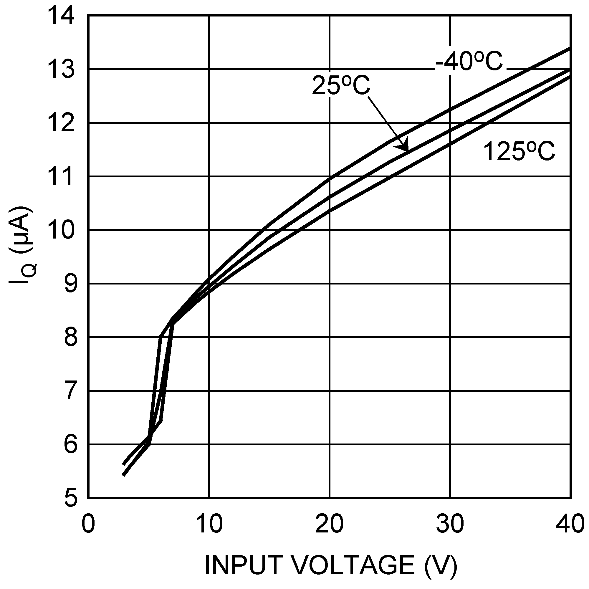
Figure 1. IQ vs Input Voltage (Shutdown)
LM3478Q-Q1 10135535.png
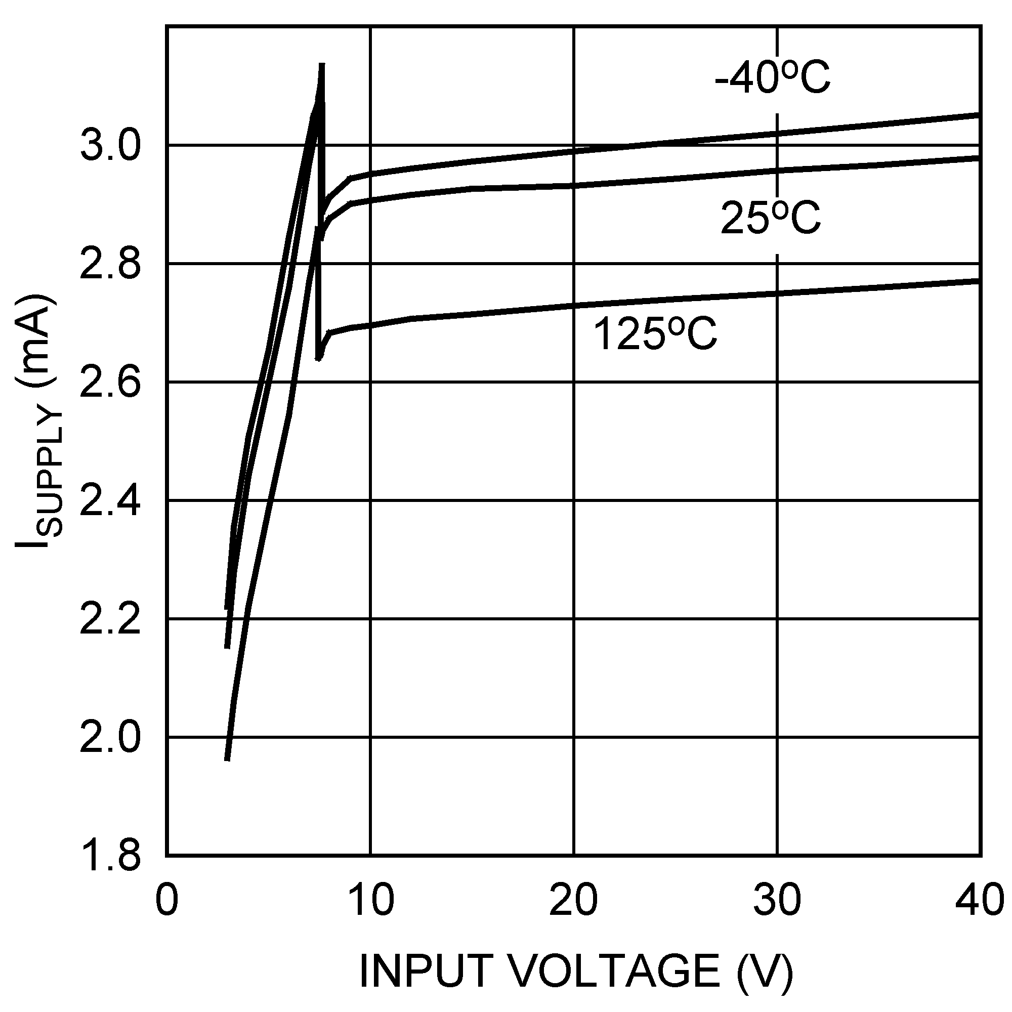
Figure 3. ISupply vs VIN (Switching)
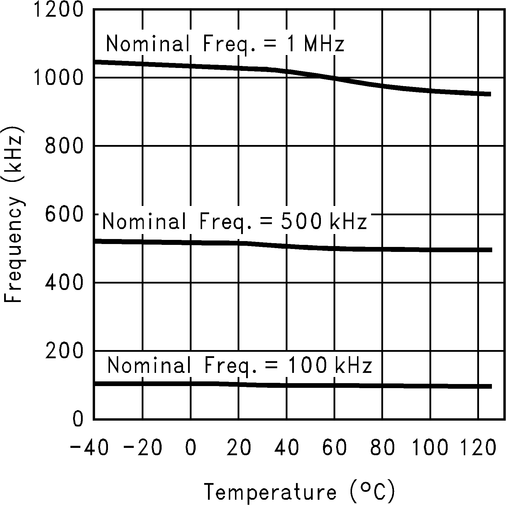
LM3478Q-Q1 10135554.png
Figure 5. Frequency vs Temperature
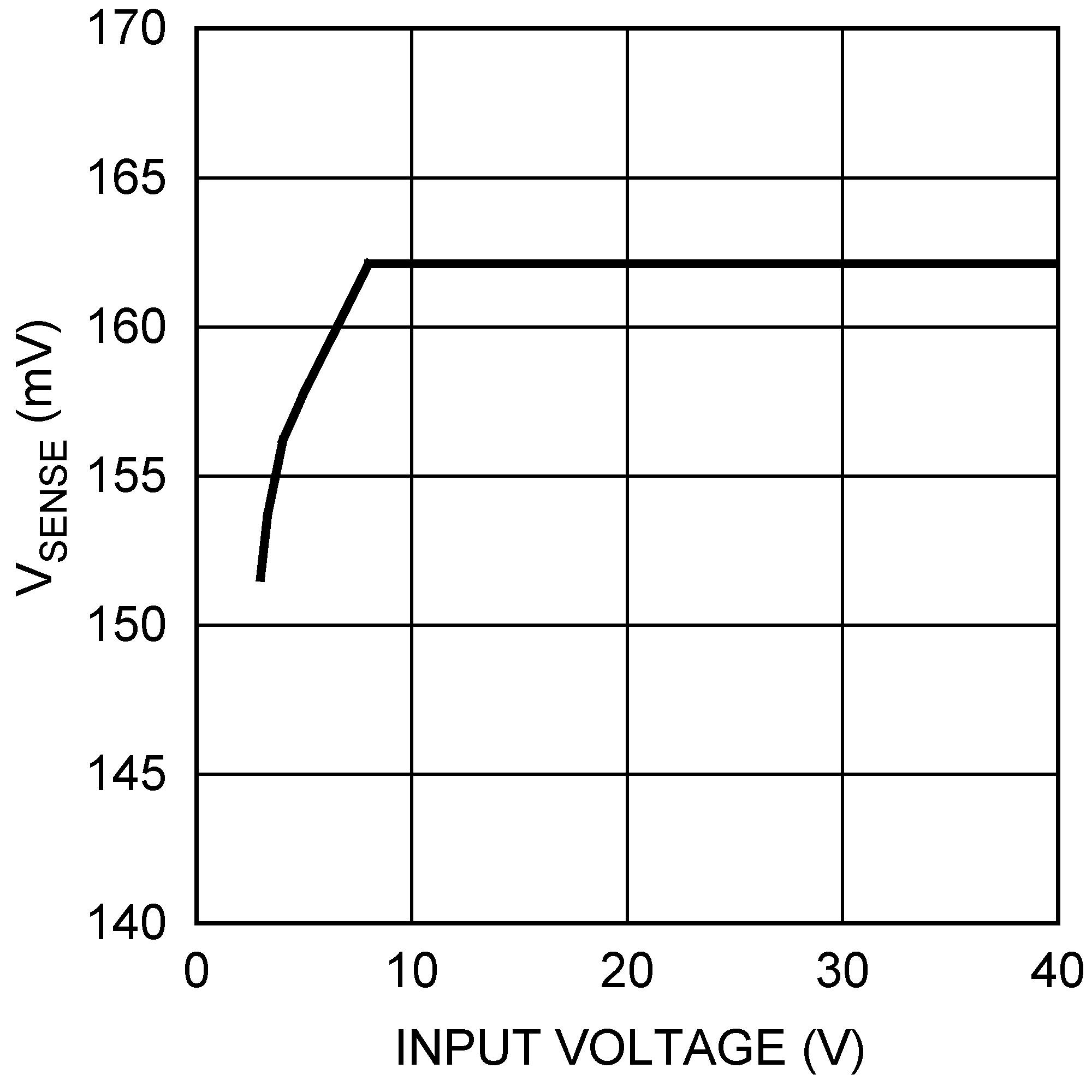
LM3478Q-Q1 10135545.png
Figure 7. Current Sense Threshold vs Input Voltage
LM3478Q-Q1 10135559.png
Figure 9. Efficiency vs Load Current (3.3-V Input and 12-V Output)
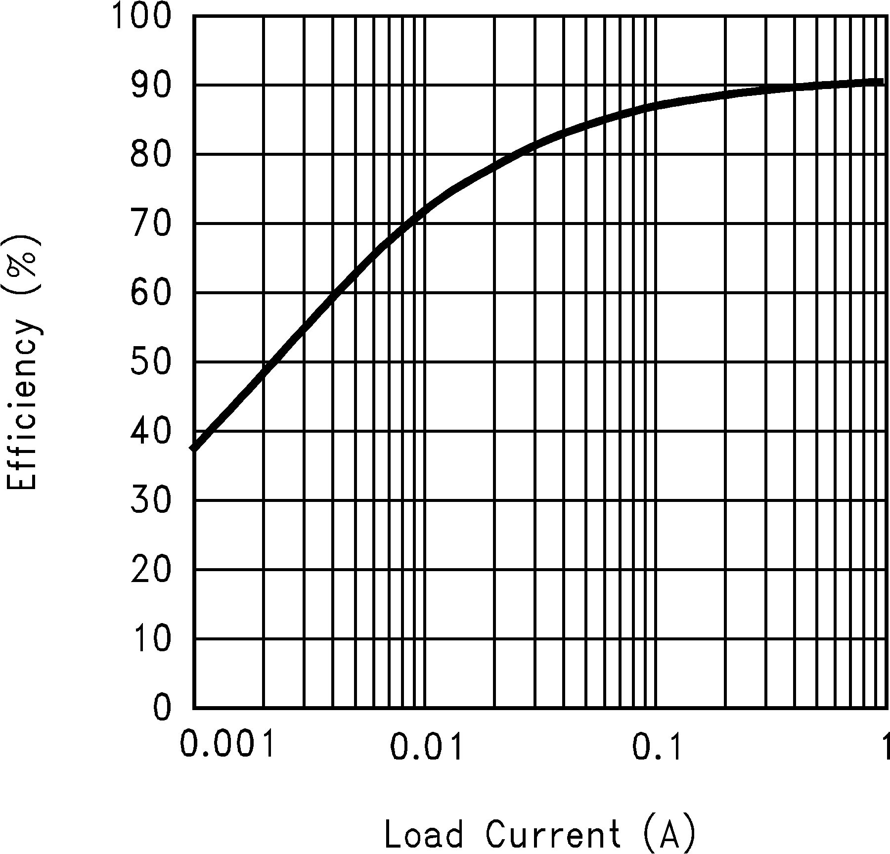
LM3478Q-Q1 10135560.png
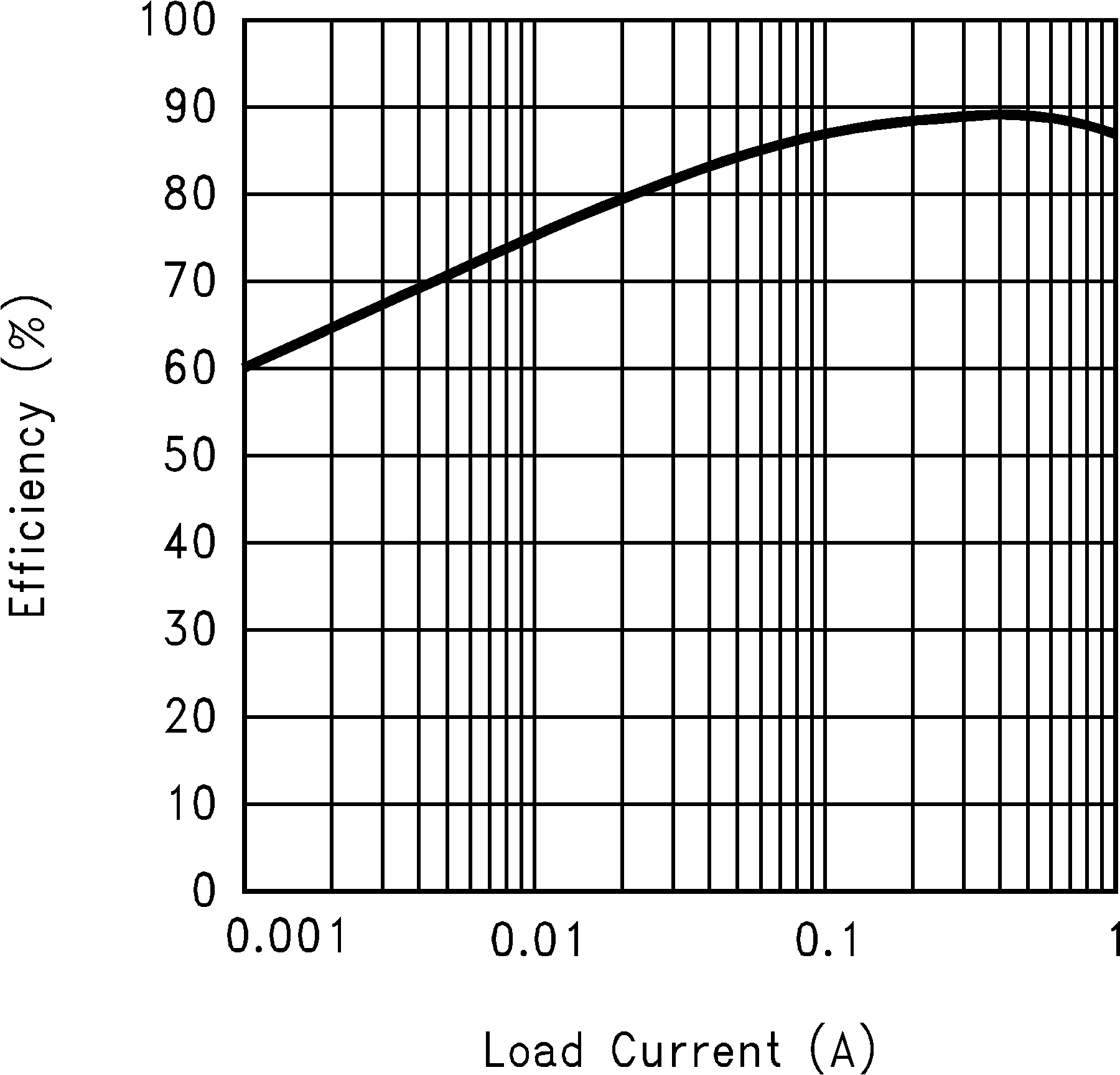
Figure 11. Efficiency vs Load Current (9-V Input and 12-V Output)
LM3478Q-Q1 10135555.png
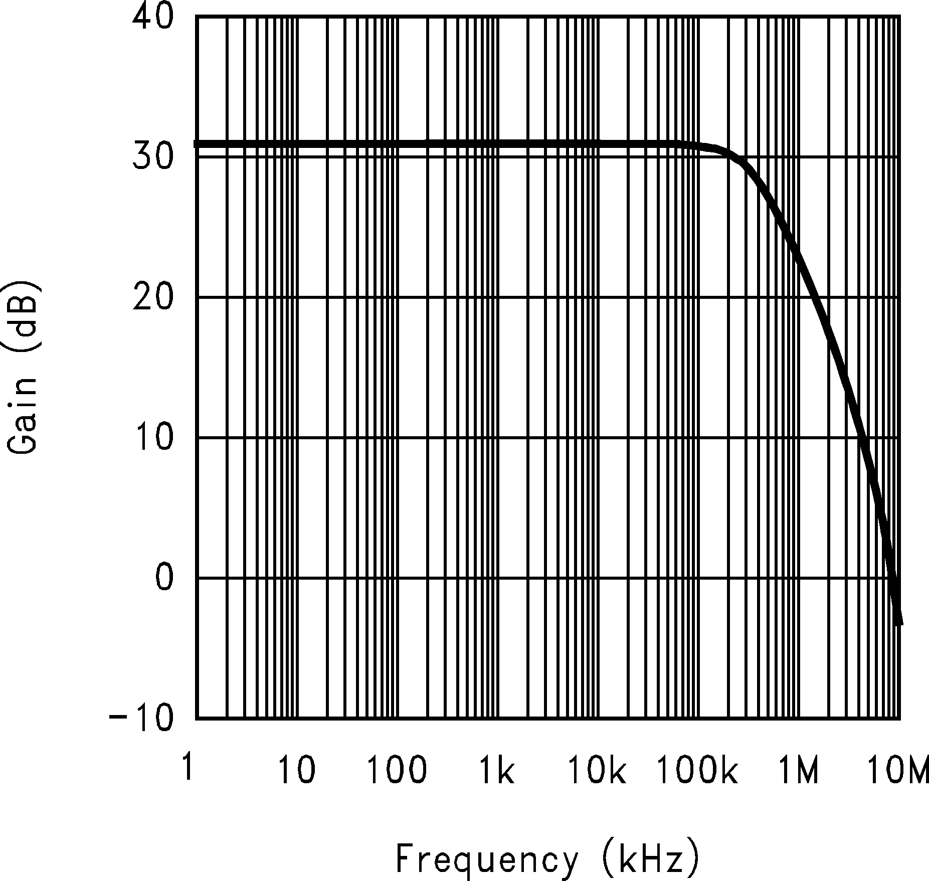
Figure 13. Error Amplifier Gain
LM3478Q-Q1 10135536.png
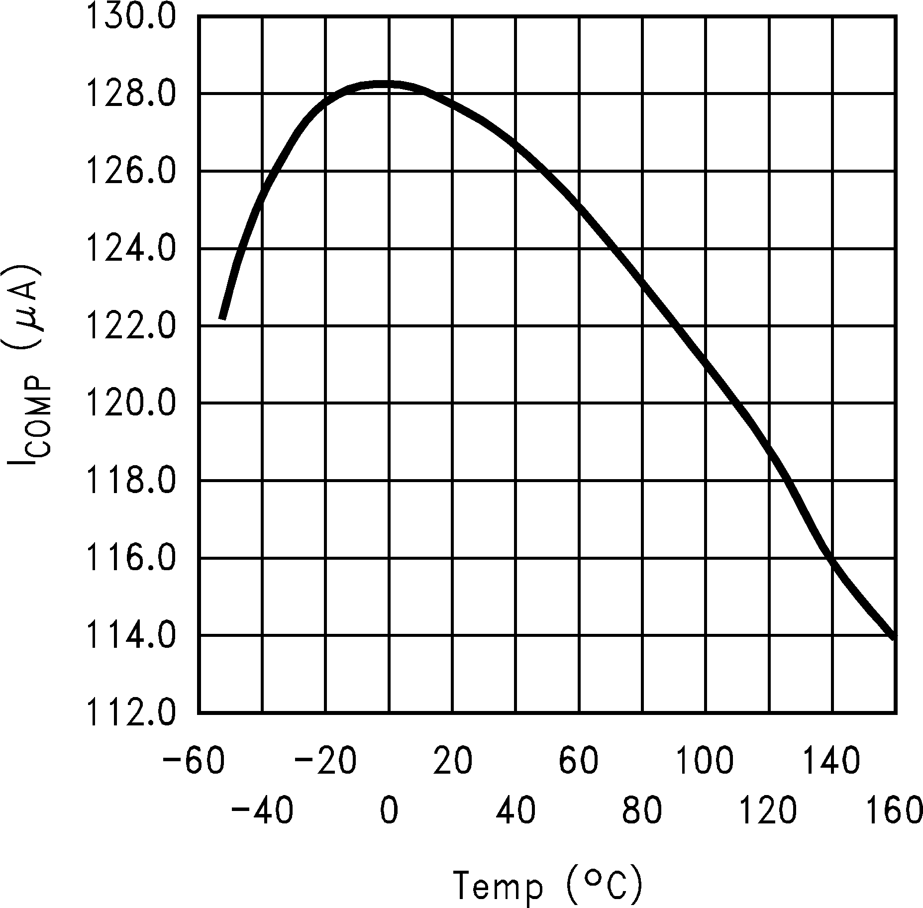
Figure 15. COMP Pin Source Current vs Temperature
LM3478Q-Q1 10135551.png
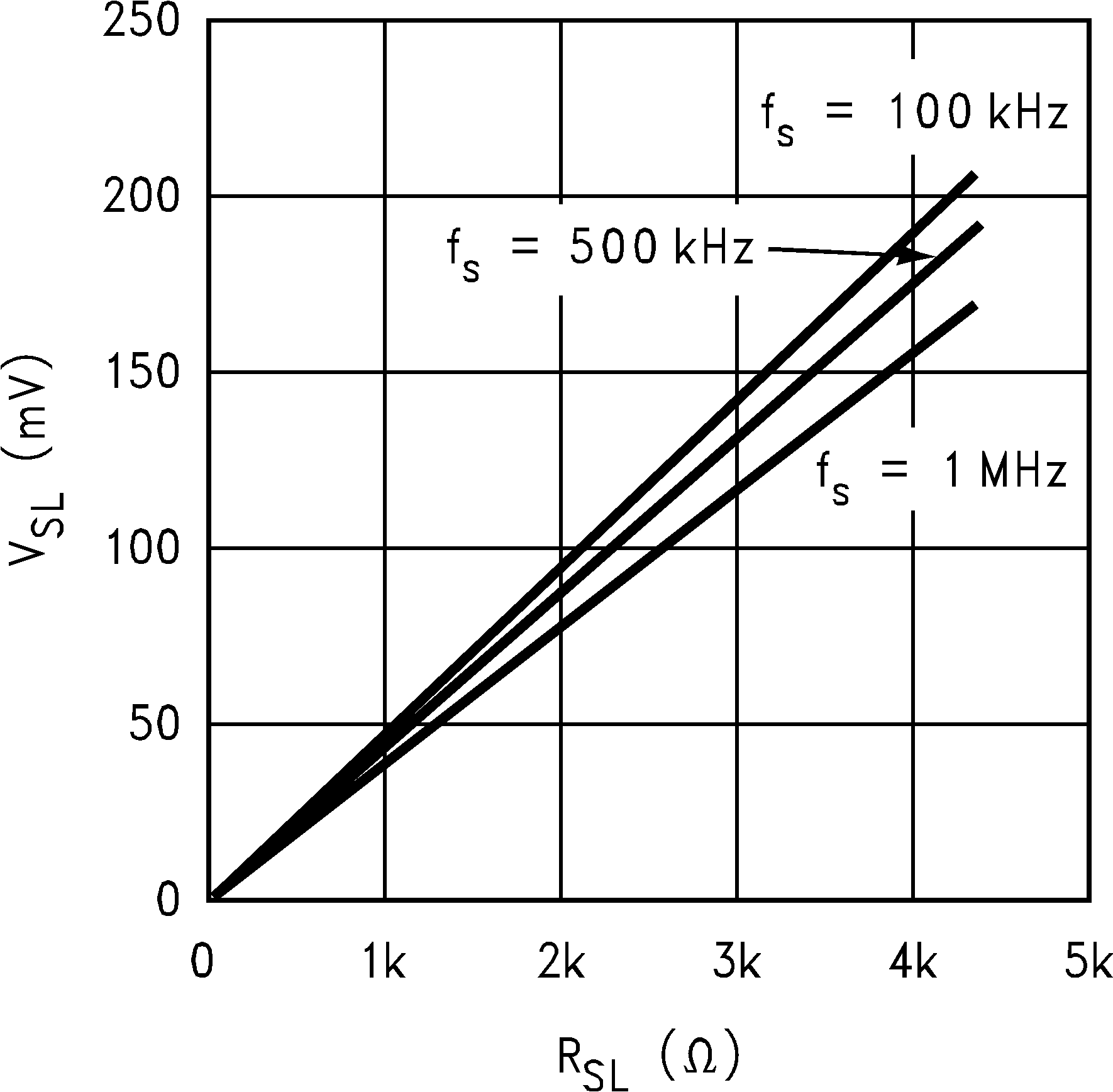
Figure 17. Compensation Ramp vs Compensation Resistor
LM3478Q-Q1 10135594.png
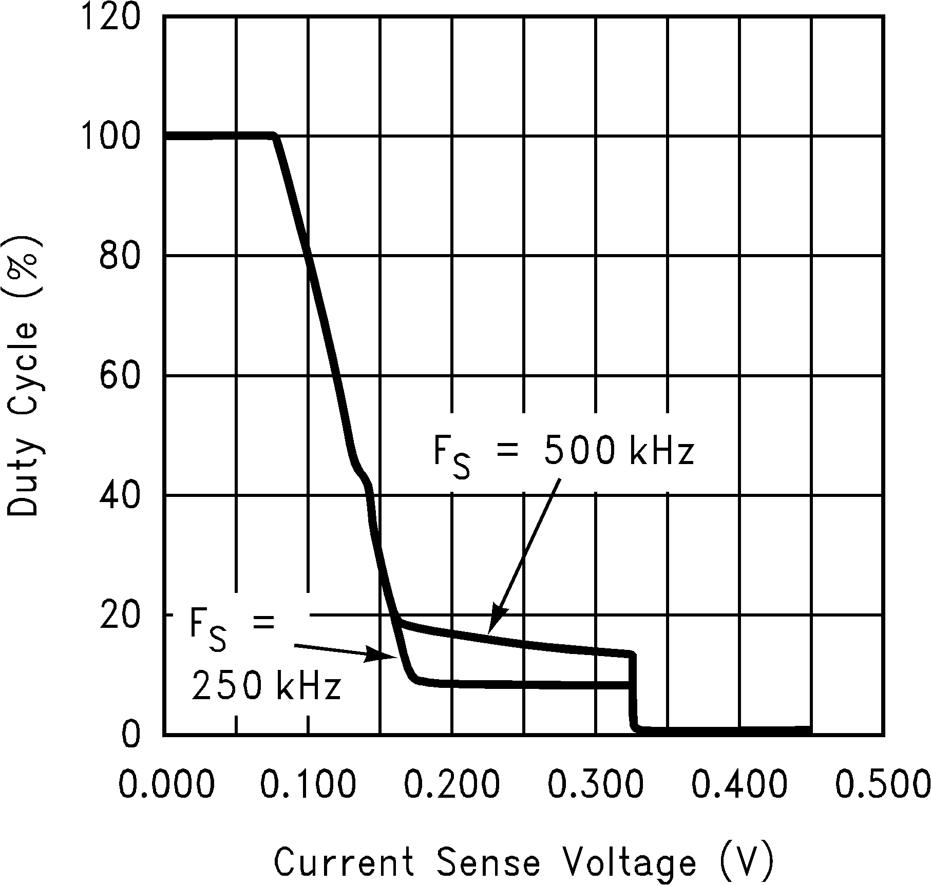
Figure 19. Duty Cycle vs Current Sense Voltage
LM3478Q-Q1 10135534.png
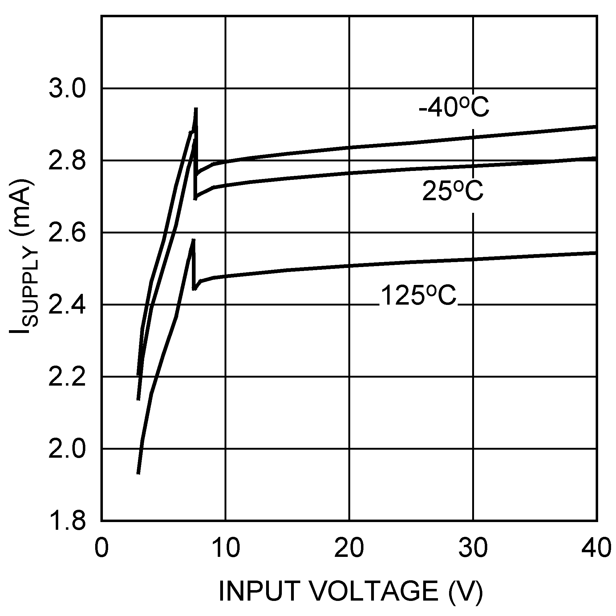
Figure 2. ISupply vs Input Voltage (Non-Switching)
LM3478Q-Q1 10135504.png
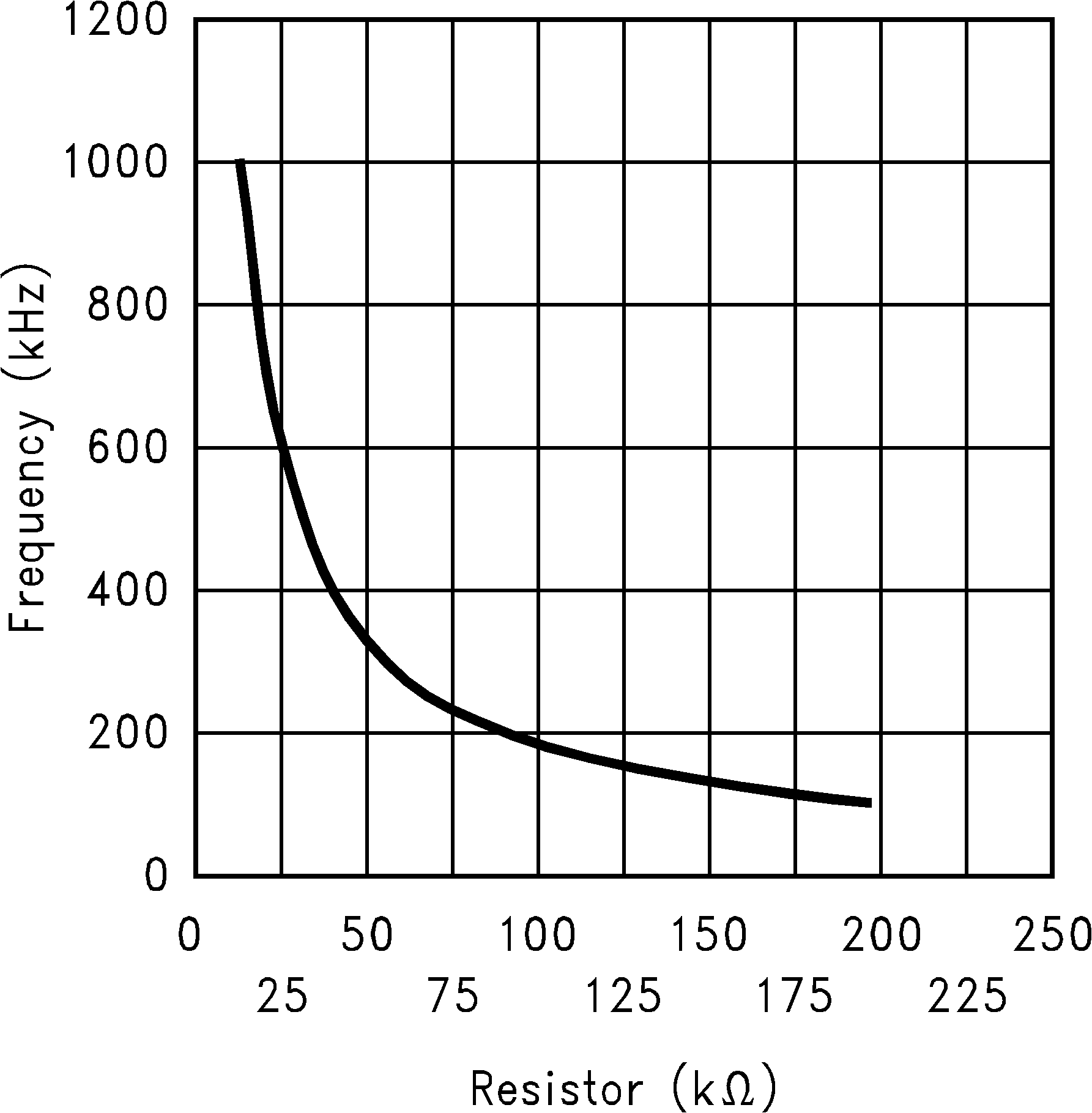
Figure 4. Switching Frequency vs RFA
LM3478Q-Q1 10135505.png
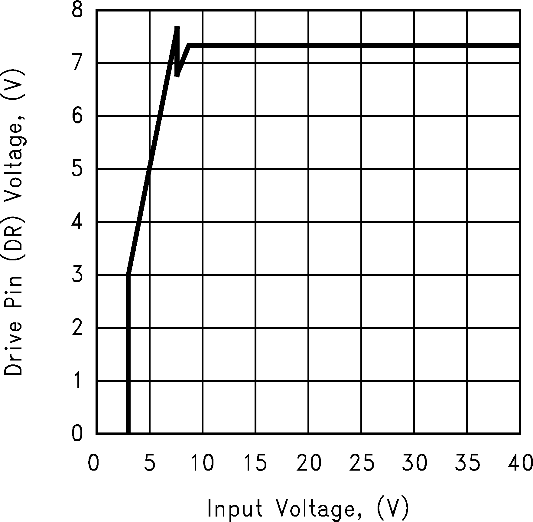
Figure 6. Drive Voltage vs Input Voltage
LM3478Q-Q1 10135562.png
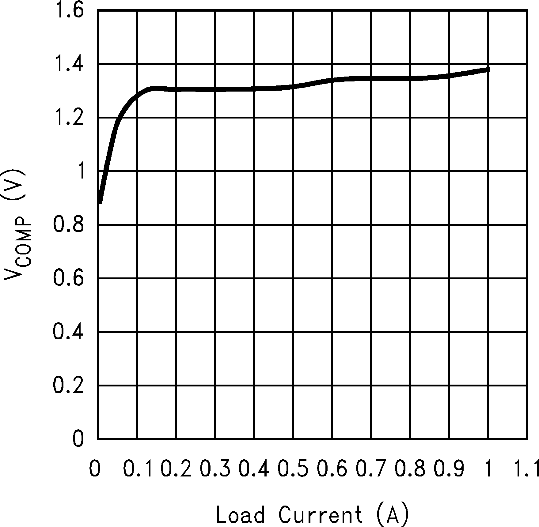
Figure 8. COMP Pin Voltage vs Load Current
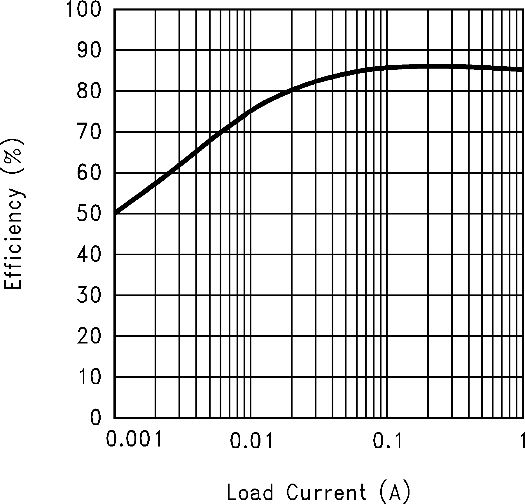
LM3478Q-Q1 10135558.png
Figure 10. Efficiency vs Load Current (5-V Input and 12-V Output)
LM3478Q-Q1 10135553.png
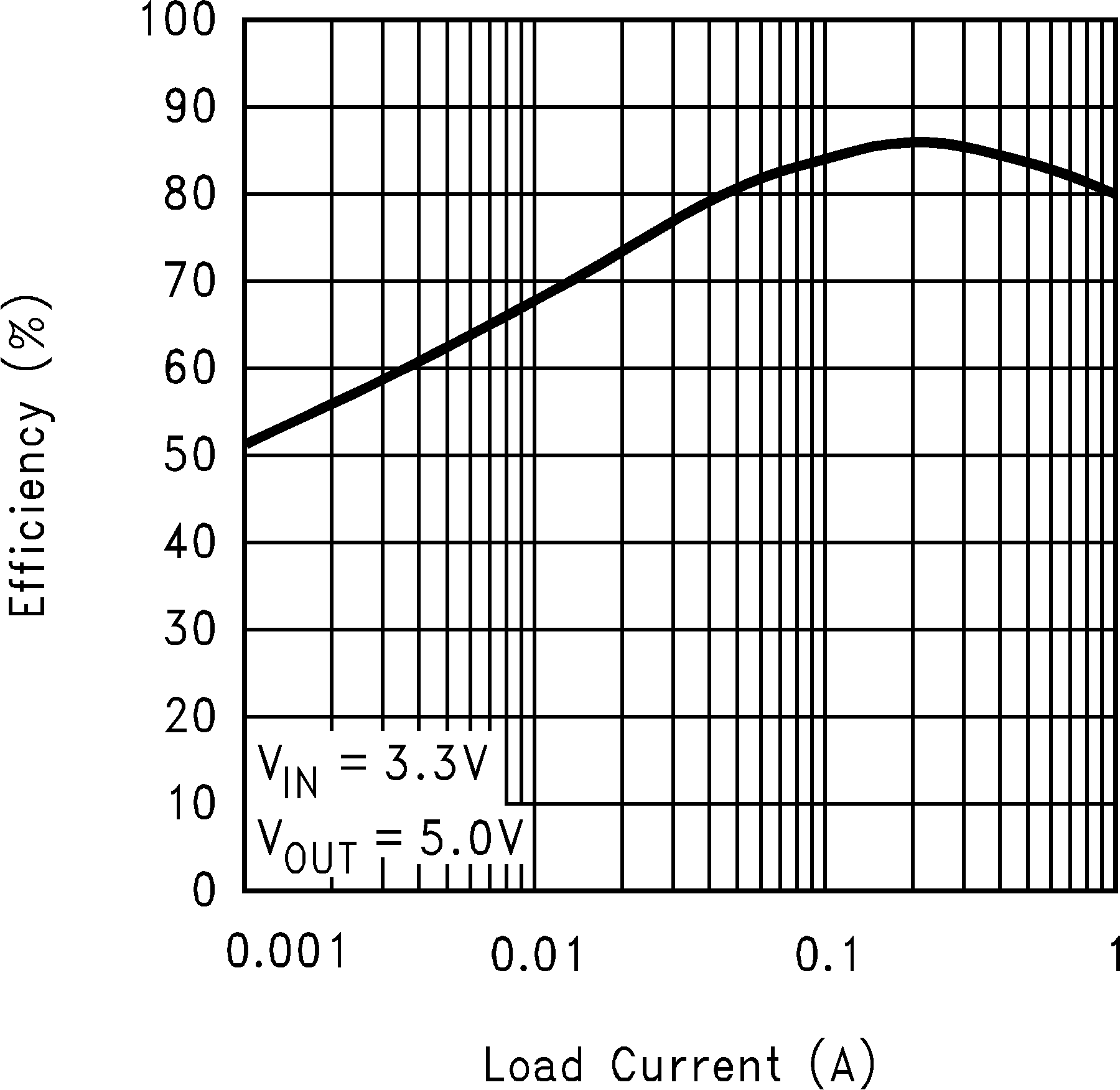
Figure 12. Efficiency vs Load Current (3.3-V Input and 5-V Output)
LM3478Q-Q1 10135556.png
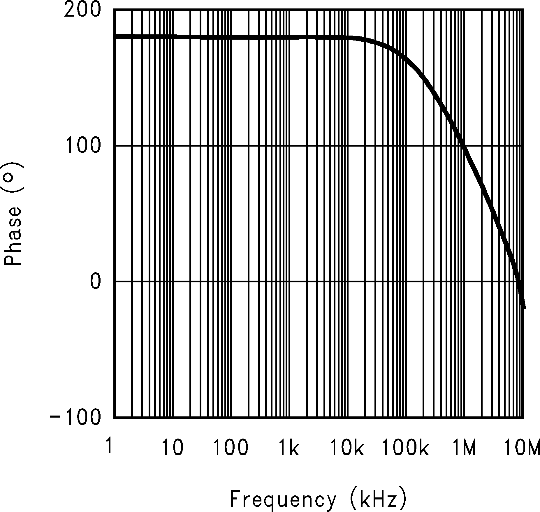
Figure 14. Error Amplifier Phase
LM3478Q-Q1 10135557.png
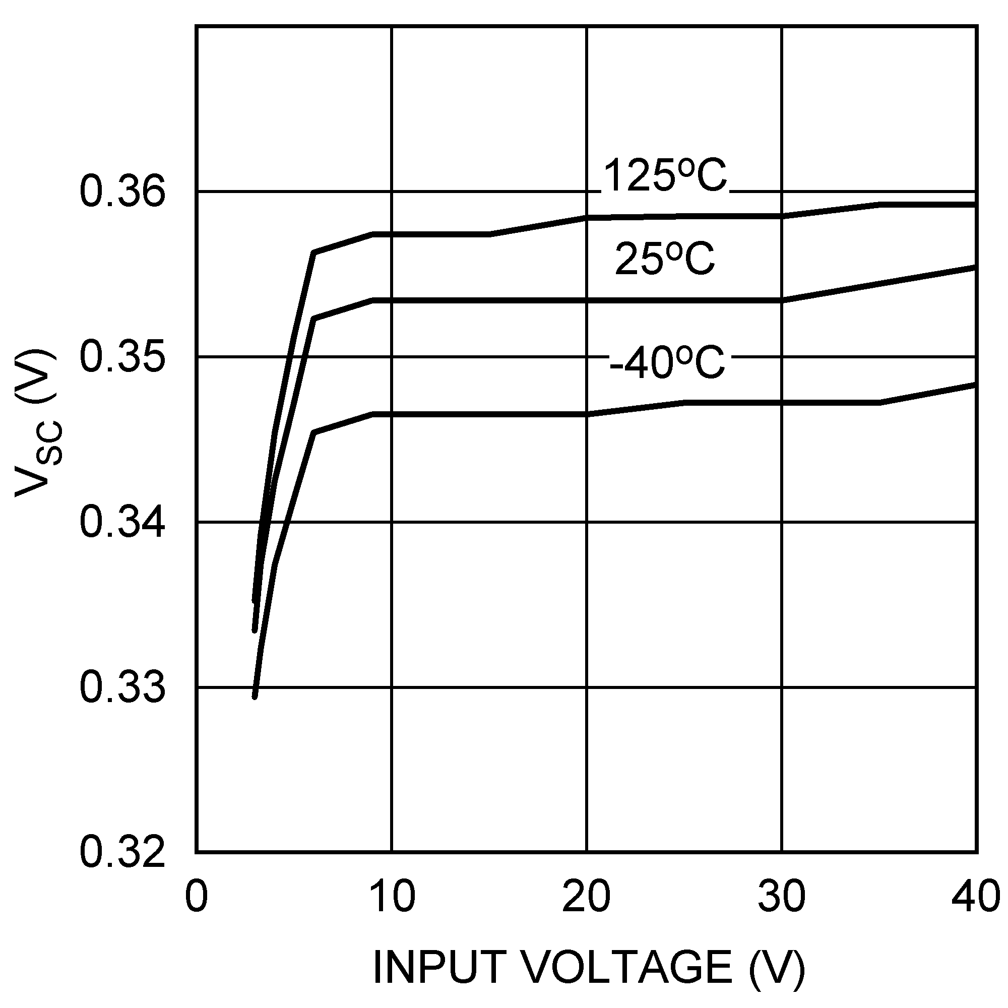
Figure 16. Short Circuit Sense Voltage vs Input Voltage
LM3478Q-Q1 10135546.png
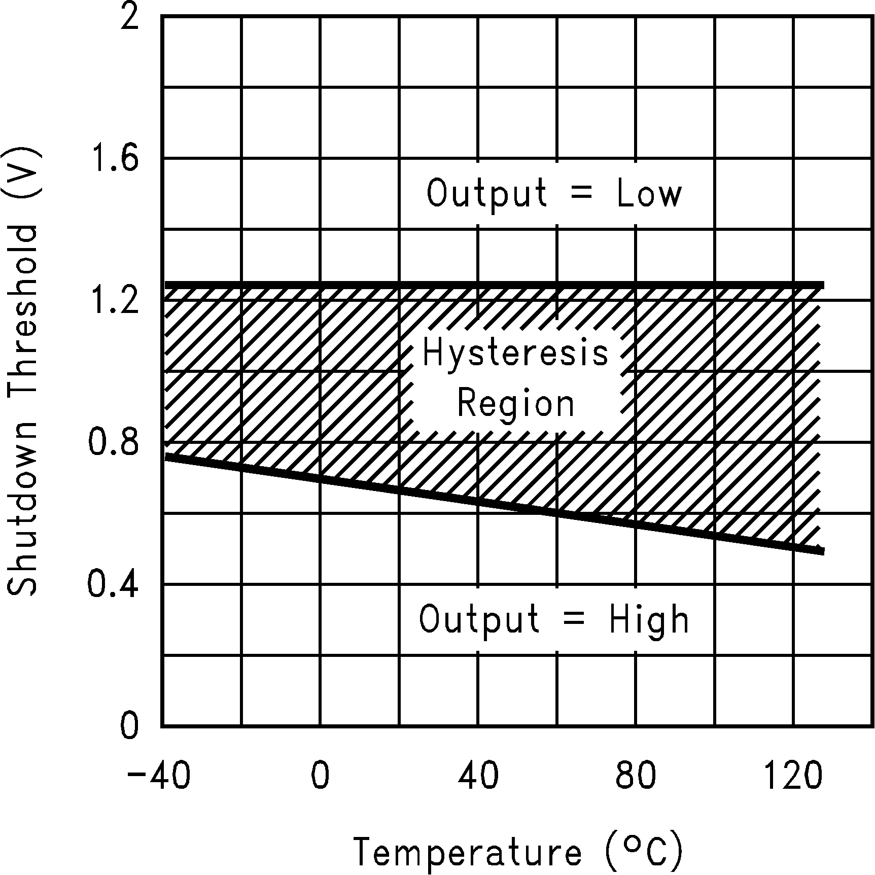
Figure 18. Shutdown Threshold Hysteresis vs Temperature