ZHCSI45 April 2018 LM3478Q-Q1
PRODUCTION DATA.
- 1 特性
- 2 应用
- 3 说明
- 4 修订历史记录
- 5 Pin Configuration and Functions
- 6 Specifications
- 7 Detailed Description
-
8 Application and Implementation
- 8.1 Application Information
- 8.2
Typical Applications
- 8.2.1
Typical High Efficiency Step-Up (Boost) Converter
- 8.2.1.1 Design Requirements
- 8.2.1.2
Detailed Design Procedure
- 8.2.1.2.1 Custom Design with WEBENCH Tools
- 8.2.1.2.2 Power Inductor Selection
- 8.2.1.2.3 Programming the Output Voltage
- 8.2.1.2.4 Setting the Current Limit
- 8.2.1.2.5 Current Limit with External Slope Compensation
- 8.2.1.2.6 Power Diode Selection
- 8.2.1.2.7 Power MOSFET Selection
- 8.2.1.2.8 Input Capacitor Selection
- 8.2.1.2.9 Output Capacitor Selection
- 8.2.1.2.10 Compensation
- 8.2.1.3 Application Curves
- 8.2.2 Typical SEPIC Converter
- 8.2.1
Typical High Efficiency Step-Up (Boost) Converter
- 9 Power Supply Recommendations
- 10Layout
- 11器件和文档支持
- 12机械、封装和可订购信息
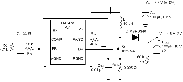
8.2.1 Typical High Efficiency Step-Up (Boost) Converter
 Figure 27. Typical High Efficiency Step-Up (Boost) Converter Schematic
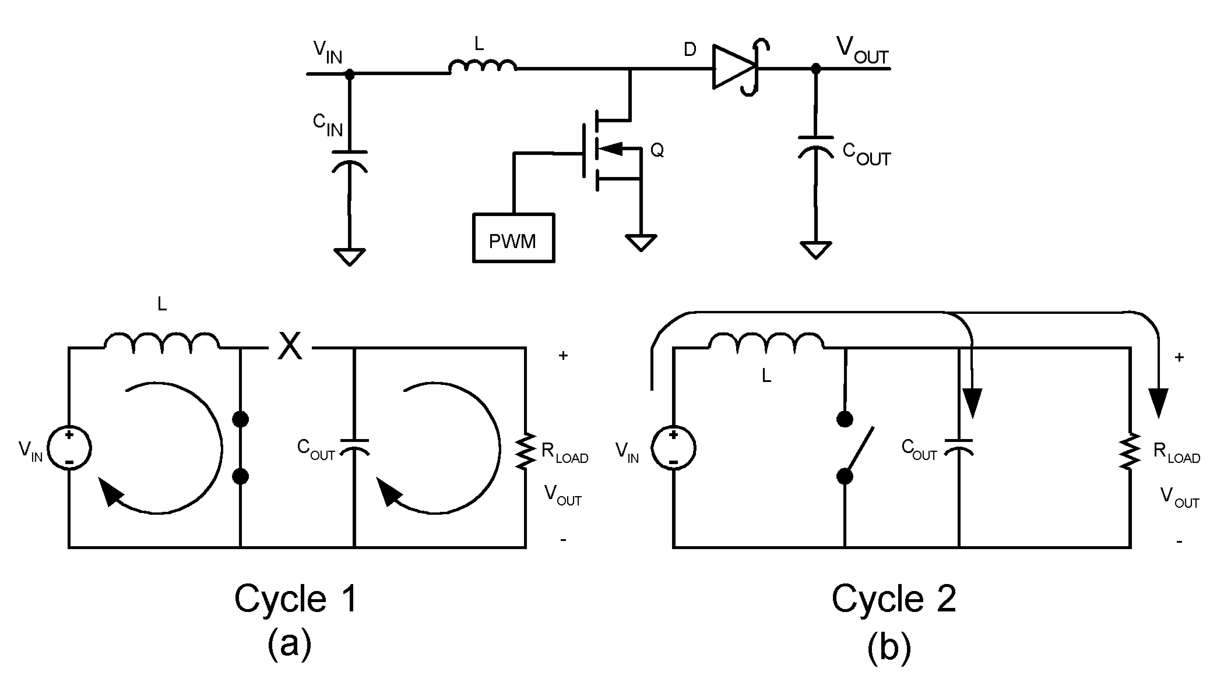
The boost converter converts a low input voltage into a higher output voltage. The basic configuration for a boost converter is shown in Figure 28. In the CCM (when the inductor current never reaches zero at steady state), the boost regulator operates in two states. In the first state of operation, MOSFET Q is turned on and energy is stored in the inductor. During this state, diode D is reverse biased and load current is supplied by the output capacitor, COUT.
In the second state, MOSFET Q is off and the diode is forward biased. The energy stored in the inductor is transferred to the load and the output capacitor. The ratio of the switch on time to the total period is the duty cycle D as shown in Equation 8.
Including the voltage drop across the MOSFET and the diode the definition for the duty cycle is shown in Equation 9.
Vd is the forward voltage drop of the diode and Vq is the voltage drop across the MOSFET when it is on.
