SNVS011H June 1999 – September 2015 LM3480
PRODUCTION DATA.
8 Application and Implementation
NOTE
Information in the following applications sections is not part of the TI component specification, and TI does not warrant its accuracy or completeness. TI’s customers are responsible for determining suitability of components for their purposes. Customers should validate and test their design implementation to confirm system functionality.
8.1 Application Information
The LM3480 is a linear voltage regulator with 1.2-V ensured maximum dropout and 100-mA ensured minimum load current. This device has 3.3-V, 5-V, 12-V, and 15-V versions. The implementation of LM3480 is discussed in this section.
8.2 Typical Application
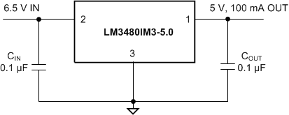
8.2.1 Design Requirements
| DESIGN PARAMETER | EXAMPLE VALUE |
|---|---|
| Input voltage | 6.5 V |
| Output voltage | 5 V |
| Output current | 100 mA |
8.2.2 Detailed Design Procedure
8.2.2.1 External Capacitors
A minimum input and output capacitance value of 0.1 µF is required for stability and adequate transient performance. There is no specific ESR limitation, although excessively high ESR will compromise transient performance. There is no specific limitation on a maximum capacitance value on the input or the output.
8.2.3 Application Curves
Unless indicated otherwise, VIN = 6.5 V, VOUT = 5 V, COUT = 0.1 µF, and TA = 25°C
 Figure 18. Line Transient Response
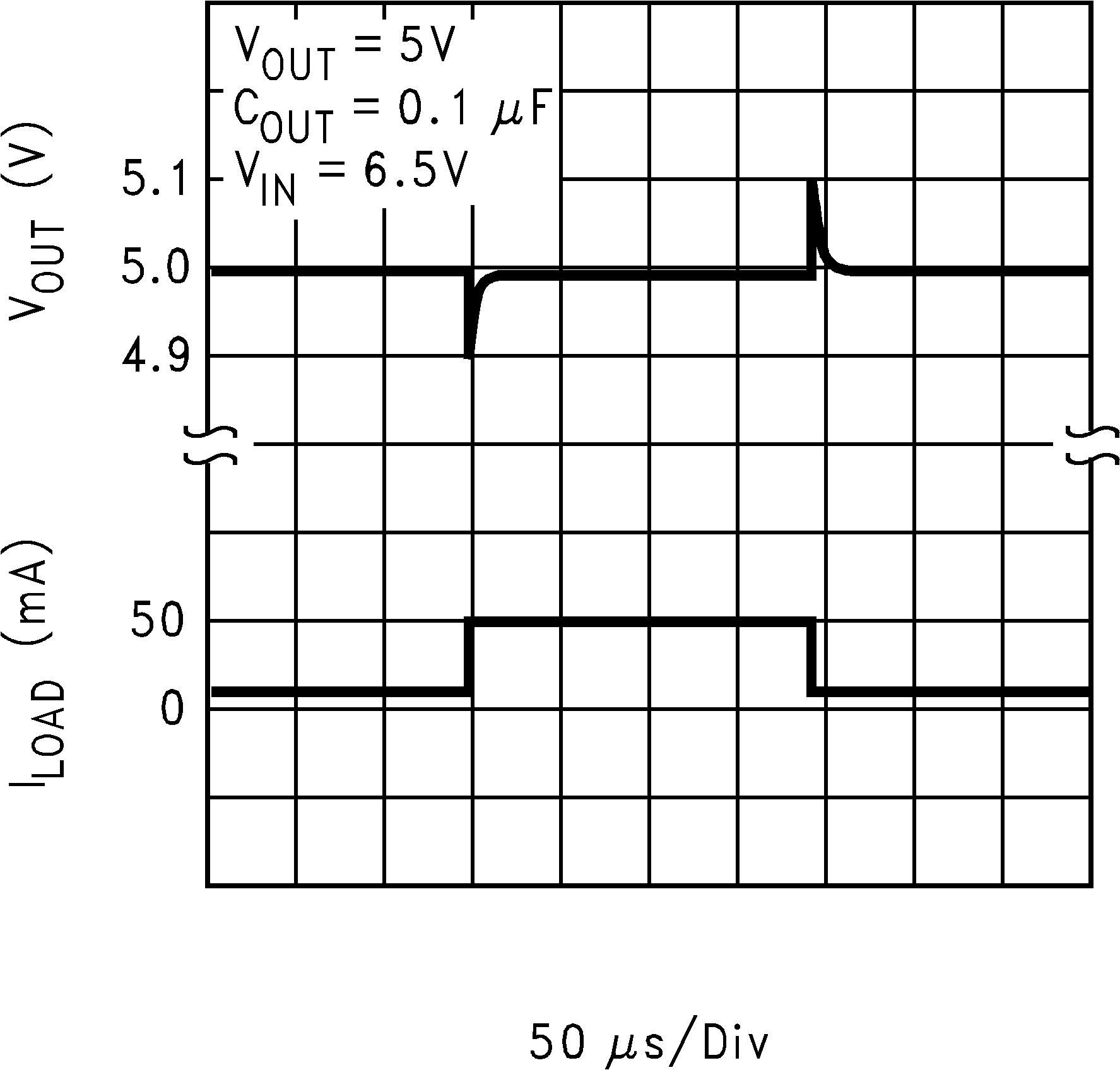 Figure 20. Load Transient Response
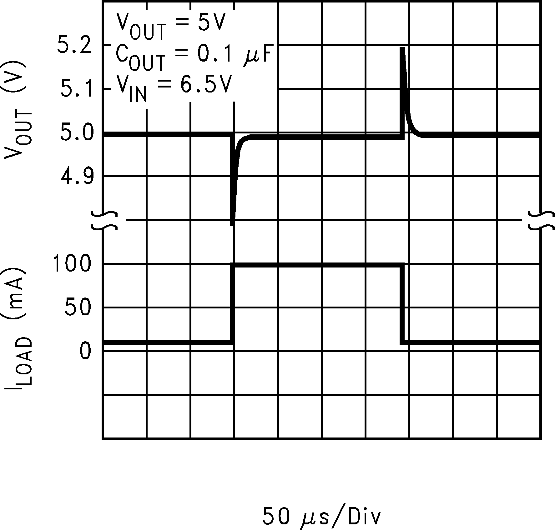 Figure 22. Load Transient Response
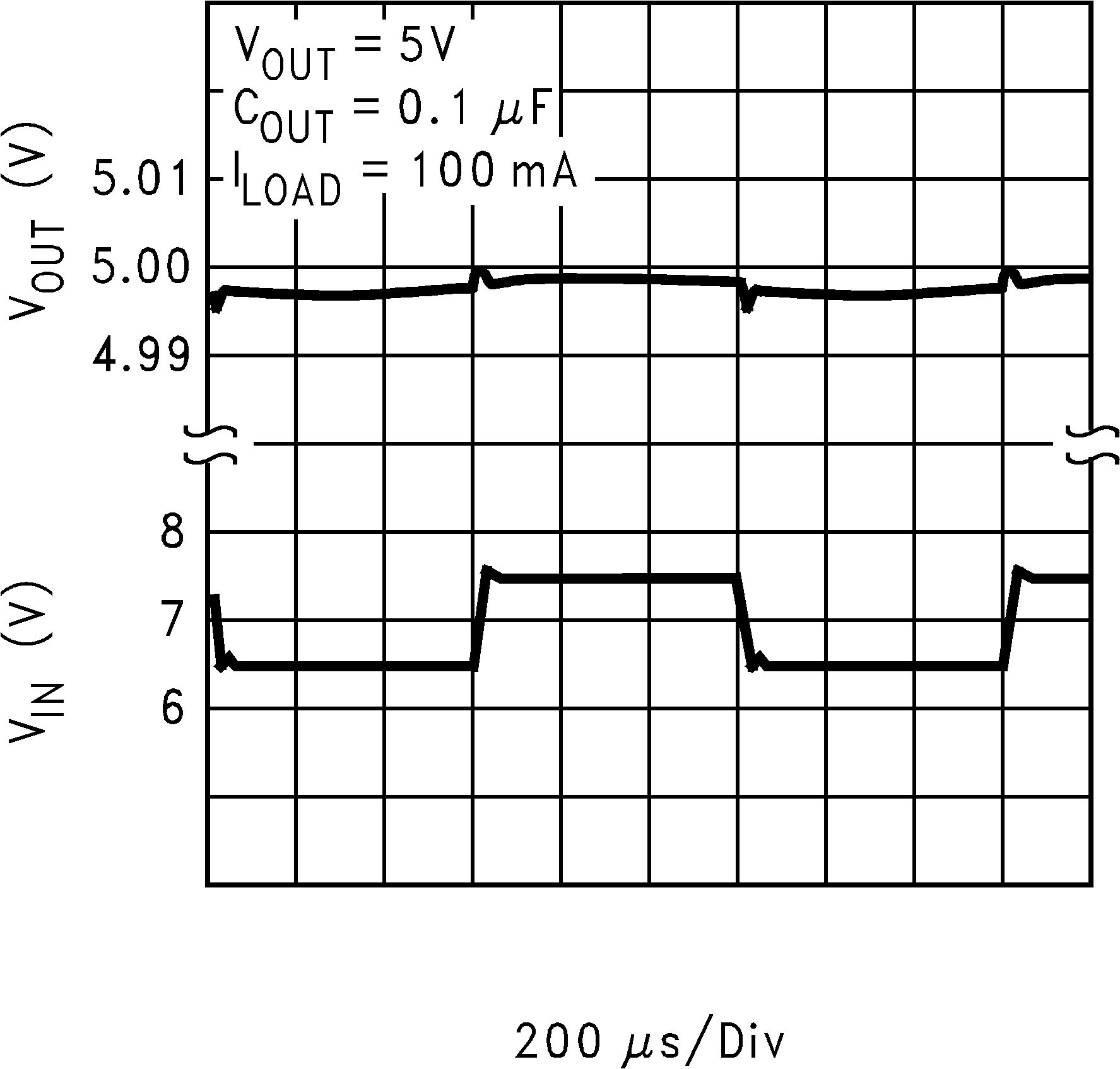 Figure 19. Line Transient Response
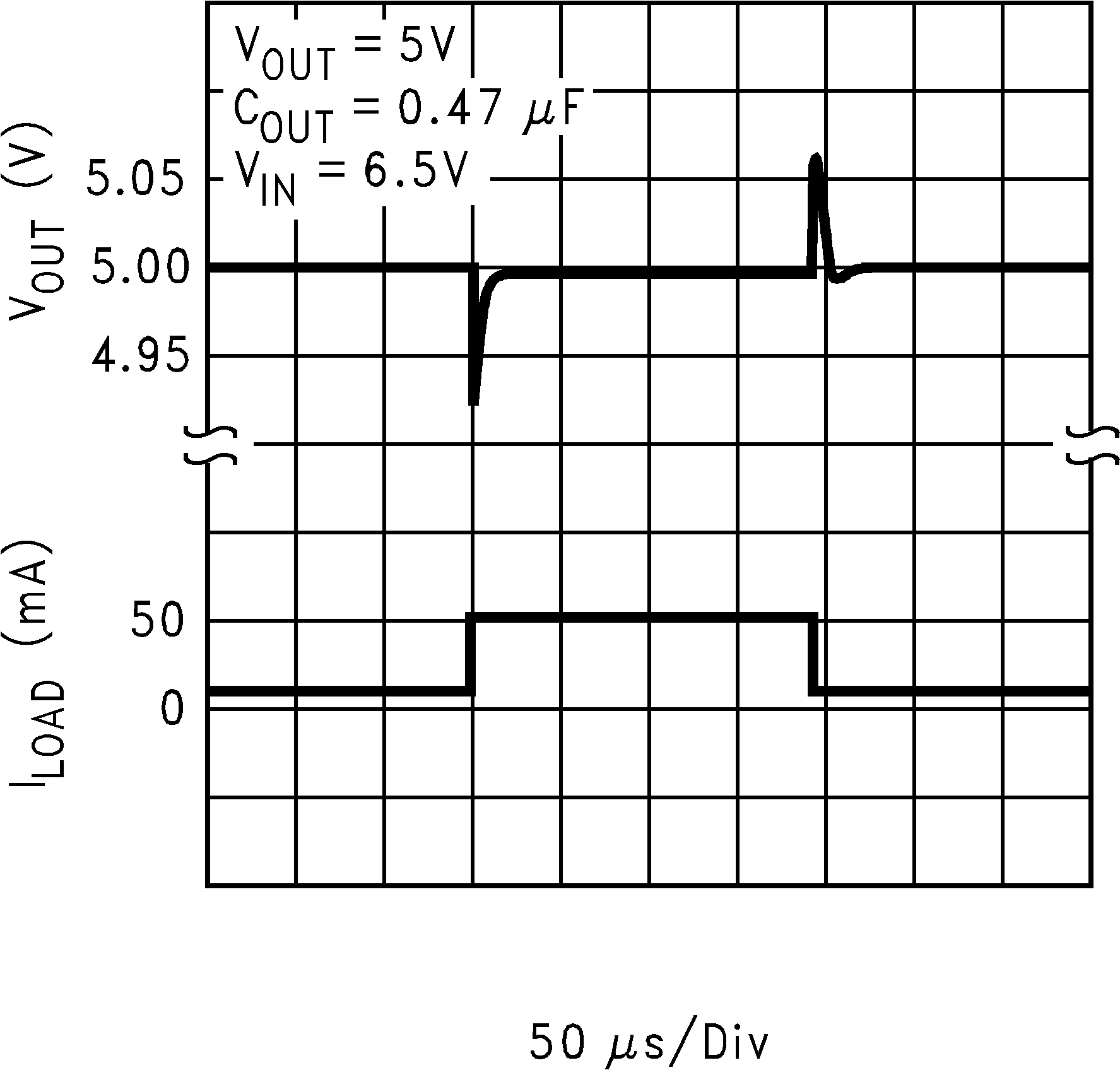 Figure 21. Load Transient Response
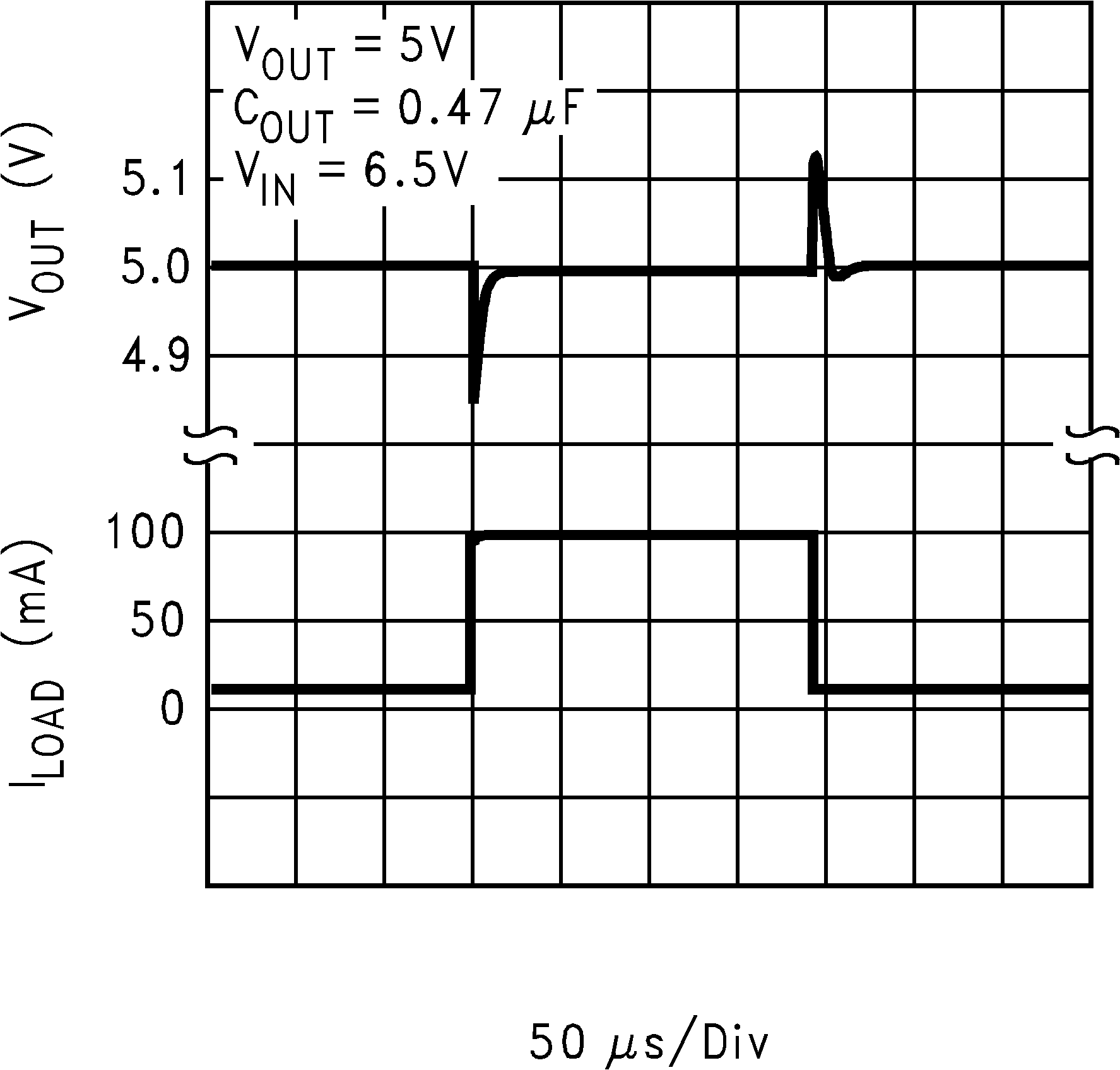 Figure 23. Load Transient Response