SNVS178H January 2002 – December 2015 LM3485
PRODUCTION DATA.
- 1 Features
- 2 Applications
- 3 Description
- 4 Revision History
- 5 Pin Configuration and Functions
- 6 Specifications
- 7 Detailed Description
-
8 Application and Implementation
- 8.1 Application Information
- 8.2
Typical Application
- 8.2.1 Design Requirements
- 8.2.2
Detailed Design Procedure
- 8.2.2.1 Step by Step Design Procedure
- 8.2.2.2 Inductor Selection (L1)
- 8.2.2.3 Output Voltage Set Point
- 8.2.2.4 Output Capacitor Selection (COUT)
- 8.2.2.5 Input Capacitor Selection (CIN)
- 8.2.2.6 Programming the Current Limit (RADJ)
- 8.2.2.7 Catch Diode Selection (D1)
- 8.2.2.8 P-Channel MOSFET Selection (Q1)
- 8.2.3 Application Curves
- 9 Power Supply Recommendations
- 10Layout
- 11Device and Documentation Support
- 12Mechanical, Packaging, and Orderable Information
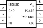
5 Pin Configuration and Functions
DGK Package
8-Pin VSSOP
Top View

Pin Functions
| NO. | NAME | I/O | DESCRIPTION |
|---|---|---|---|
| 1 | ISENSE | I | The current sense input pin. This pin should be connected to Drain node of the external PFET. |
| 2 | GND | G | Signal ground |
| 3 | NC | — | No connection |
| 4 | FB | I | The feedback input. Connect the FB to a resistor voltage divider between the output and GND for an adjustable output voltage. |
| 5 | ADJ | I | Current limit threshold adjustment. It connects to an internal 5.5-µA current source. A resistor is connected between this pin and the input Power Supply. The voltage across this resistor is compared with the VDS of the external PFET to determine if an over-current condition has occurred. |
| 6 | PWR GND | G | Power ground |
| 7 | PGATE | O | Gate Drive output for the external PFET. PGATE swings between VIN and VIN-5 V. |
| 8 | VIN | P/I | Power supply input pin |