SNVS443C May 2006 – December 2016 LM3489 , LM3489-Q1
PRODUCTION DATA.
- 1 Features
- 2 Applications
- 3 Description
- 4 Revision History
- 5 Pin Configuration and Functions
- 6 Specifications
- 7 Detailed Description
- 8 Application and Implementation
- 9 Power Supply Recommendations
- 10Layout
- 11Device and Documentation Support
- 12Mechanical, Packaging, and Orderable Information
6 Specifications
6.1 Absolute Maximum Ratings
See (1).| MIN | MAX | UNIT | ||
|---|---|---|---|---|
| VIN voltage | –0.3 | 36 | V | |
| PGATE voltage | –0.3 | 36 | V | |
| FB voltage | –0.3 | 5 | V | |
| ISENSE voltage | –1 | 36 | V | |
| –1 (<100 ns) | ||||
| ADJ voltage | –0.3 | 36 | V | |
| EN voltage(2) | –0.3 | 6 | V | |
| Power dissipation, TA = 25°C(3) | 417 | mW | ||
| Junction temperature, TJ | –40 | 150 | °C | |
| Storage temperature, Tstg | –65 | 150 | °C | |
(1) Stresses beyond those listed under Absolute Maximum Ratings may cause permanent damage to the device. These are stress ratings only, which do not imply functional operation of the device at these or any other conditions beyond those indicated under Recommended Operating Conditions. Exposure to absolute-maximum-rated conditions for extended periods may affect device reliability.
(2) This pin is internally pulled high and clamped at 8 V (typical). The absolute maximum and operating maximum rating specifies the input level allowed for an external voltage source applied to this pin without triggering the internal clamp with margin.
(3) The maximum allowable power dissipation is a function of the maximum junction temperature, TJ_MAX, the junction-to-ambient thermal resistance, RθJA and the ambient temperature, TA. The maximum allowable power dissipation at any ambient temperature is calculated using: PD= (TJ – TA) / RθJA. Exceeding the maximum allowable power dissipation will lead to excessive die temperature.
6.2 ESD Ratings: LM3489
| VALUE | UNIT | |||
|---|---|---|---|---|
| V(ESD) | Electrostatic discharge | Human-body model (HBM), per ANSI/ESDA/JEDEC JS-001(1) | ±2000 | V |
| Charged-device model (CDM), per JEDEC specification JESD22-C101(2) | ±750 | |||
(1) JEDEC document JEP155 states that 500-V HBM allows safe manufacturing with a standard ESD control process.
(2) JEDEC document JEP157 states that 250-V CDM allows safe manufacturing with a standard ESD control process.
6.3 ESD Ratings: LM3489-Q1
| VALUE | UNIT | |||
|---|---|---|---|---|
| V(ESD) | Electrostatic discharge | Human body model (HBM), per AEC Q100-002(1) | ±2000 | V |
| Charged device model (CDM), per AEC Q100-011 | ±750 | |||
6.4 Recommended Operating Conditions
over operating free-air temperature range (unless otherwise noted)| MIN | MAX | UNIT | |||
|---|---|---|---|---|---|
| VIN | Supply voltage | 4.5 | 35 | V | |
| EN voltage(1) | 5.5 | V | |||
| TJ | Operating junction temperature(2) | LM3489 | –40 | 125 | °C |
| LM3489-Q1 | –40 | 150 | °C | ||
(1) This pin is internally pulled high and clamped at 8 V (typical). The absolute maximum and operating maximum rating specifies the input level allowed for an external voltage source applied to this pin without triggering the internal clamp with margin.
(2) High junction temperatures degrade operating lifetimes. Operating lifetime is de-rated for junction temperatures greater than 125°C.
6.5 Thermal Information
| THERMAL METRIC(1) | LM3489 | UNIT | |
|---|---|---|---|
| DGK (VSSOP) | |||
| 8 PINS | |||
| RθJA | Junction-to-ambient thermal resistance | 163.7 | °C/W |
| RθJC(top) | Junction-to-case (top) thermal resistance | 56.6 | °C/W |
| RθJB | Junction-to-board thermal resistance | 83.3 | °C/W |
| ψJT | Junction-to-top characterization parameter | 5.4 | °C/W |
| ψJB | Junction-to-board characterization parameter | 82 | °C/W |
| RθJC(bot) | Junction-to-case (bottom) thermal resistance | — | °C/W |
(1) For more information about traditional and new thermal metrics, see the Semiconductor and IC Package Thermal Metrics application report.
6.6 Electrical Characteristics
Typical values correspond to TJ = 25°C. Minimum and maximum limits apply over TJ = –40°C to 125°C for the LM3489 and LM3489-Q1. VIN = 12 V, VISNS = VIN − 1 V, and VADJ = VIN − 1.1 V (unless otherwise noted).| PARAMETER | TEST CONDITIONS | MIN | TYP | MAX | UNIT | ||
|---|---|---|---|---|---|---|---|
| ISHDN | Shutdown input supply current | EN = 0 V | 7 | 15 | µA | ||
| VEN | Enable threshold voltage | Enable rising | 1.15 | 1.5 | 1.85 | V | |
| VEN_HYST | Enable threshold hysteresis | 130 | mV | ||||
| IQ | Quiescent current at ground pin | FB = 1.5 V (not switching) | 280 | 400 | µA | ||
| VFB | Feedback voltage(1) | 1.214 | 1.239 | 1.264 | V | ||
| VHYST | Comparator hysteresis | 10 | 20 | mV | |||
| VCL_OFFSET | Current limit comparator offset | VFB = 1 V | –20 | 0 | 20 | mV | |
| ICL_ADJ | Current limit ADJ current source | VFB = 1.5 V | 3 | 5.5 | 7 | µA | |
| TCL | Current limit one-shot off-time | VADJ = 11.5 V, VISNS = 11 V, VFB = 1 V | 6 | 9 | 14 | µs | |
| RPGATE | Driver resistance | Source, ISOURCE = 100 mA | 5.5 | Ω | |||
| Sink, ISINK = 100 mA | 8.5 | ||||||
| IPGATE | Driver output current | Source, VIN = 7 V, PGATE = 3.5 V | 0.44 | A | |||
| Sink, VIN = 7 V, PGATE = 3.5 V | 0.1 | ||||||
| IFB | FB pin bias current(2) | VFB = 1 V | 300 | 750 | nA | ||
| TONMIN_NOR | Minimum ON time in normal operation | VISNS = VADJ + 0.1 V, Cload on OUT = 1000 pF(3) | 100 | ns | |||
| TONMIN_CL | Minimum ON time in current limit | VISNS = VADJ – 0.1 V, VFB = 1 V, Cload on OUT = 1000 pF(3) |
200 | ns | |||
| %VFB/ΔVIN | Feedback voltage line regulation | 4.5 V ≤ VIN ≤ 35 V | 0.01% | V | |||
(1) The VFB is the trip voltage at the FB pin when PGATE switches from high to low.
(2) Bias current flows out from the FB pin.
(3) A 1000-pF capacitor is connected between VIN and PGATE.
6.7 Typical Characteristics
At TA = 25°C and applicable to both LM3489 and LM3489-Q1 at VIN = 12 V with configuration in Detailed Description (unless otherwise noted).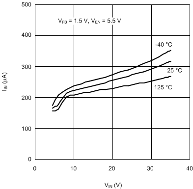 Figure 1. Quiescent Current vs Input Voltage
 Figure 3. Feedback Voltage vs Temperature
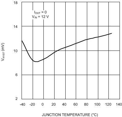 Figure 5. Feedback Voltage Hysteresis vs Temperature
 Figure 7. Current Limit One Shot OFF Time vs Temperature
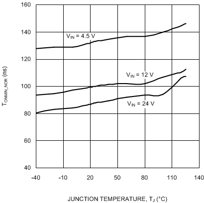 Figure 9. Minimum ON Time
 vs Temperature (Normal Operation)
 Figure 11. Operating ON Time vs Load Current

VOUT = 5 V, L = 22 µH
Figure 13. Efficiency vs Load Current
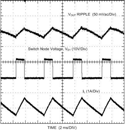
VIN = 12 V, VOUT = 3.3 V, IOUT = 500 mA
Figure 15. Continuous Mode Operation

VOUT = 3.3 V, 500 mA loaded
Figure 17. Enable Transient
 Figure 2. Shutdown Current vs Input Voltage
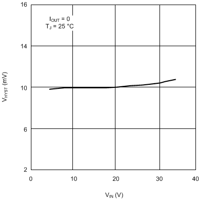 Figure 4. Feedback Voltage Hysteresis vs Input Voltage
 Figure 6. Current Limit ADJ Current vs Temperature
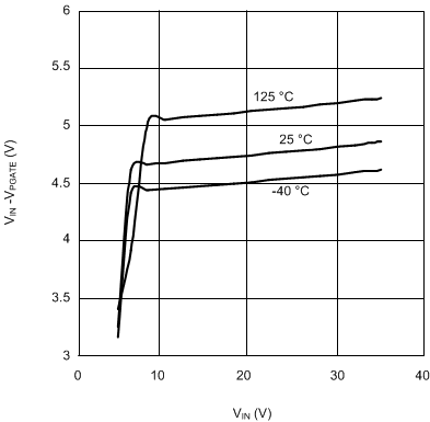 Figure 8. VIN – VPGATE vs VIN
 Figure 10. Minimum ON Time
 vs Temperature (Current Limit)
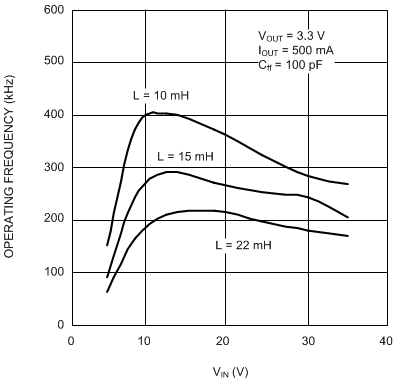 Figure 12. Operating Frequency vs Input Voltage

VOUT = 5 V, L = 22 µH
Figure 14. VOUT Regulation vs Load Current
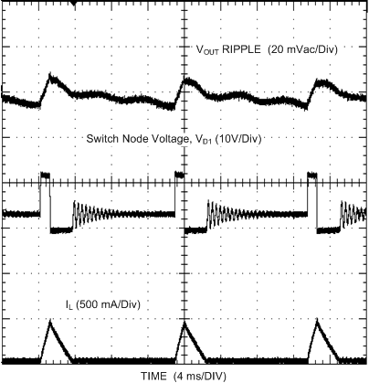
VIN = 12 V, VOUT =3.3 V, IOUT = 50 mA
Figure 16. Discontinuous Mode Operation

VOUT = 3.3 V, 500 mA loaded
Figure 18. Shutdown Transient