ZHCSD58G June 2012 – November 2017 LM34925
PRODUCTION DATA.
- 1 特性
- 2 应用
- 3 说明
- 4 修订历史记录
- 5 Pin Configuration and Functions
- 6 Specifications
-
7 Detailed Description
- 7.1 Overview
- 7.2 Functional Block Diagram
- 7.3
Feature Description
- 7.3.1 Control Overview
- 7.3.2 VCC Regulator
- 7.3.3 Regulation Comparator
- 7.3.4 Overvoltage Comparator
- 7.3.5 On-Time Generator
- 7.3.6 Current Limit
- 7.3.7 N-Channel Buck Switch and Driver
- 7.3.8 Synchronous Rectifier
- 7.3.9 Undervoltage Detector
- 7.3.10 Thermal Protection
- 7.3.11 Ripple Configuration
- 7.3.12 Soft Start
- 7.4 Device Functional Modes
-
8 Application and Implementation
- 8.1 Application Information
- 8.2
Typical Application
- 8.2.1
Application Circuit: 20-V to 95-V Input and 10-V, 100-mA Output Isolated Fly-Buck Converter
- 8.2.1.1 Design Requirements
- 8.2.1.2
Detailed Design Procedure
- 8.2.1.2.1 Transformer Turns Ratio
- 8.2.1.2.2 Total IOUT
- 8.2.1.2.3 RFB1, RFB2
- 8.2.1.2.4 Frequency Selection
- 8.2.1.2.5 Transformer Selection
- 8.2.1.2.6 Primary Output Capacitor
- 8.2.1.2.7 Secondary Output Capacitor
- 8.2.1.2.8 Type III Feedback Ripple Circuit
- 8.2.1.2.9 Secondary Diode
- 8.2.1.2.10 VCC and Bootstrap Capacitor
- 8.2.1.2.11 Input Capacitor
- 8.2.1.2.12 UVLO Resistors
- 8.2.1.2.13 VCC Diode
- 8.2.2 Application Curves
- 8.2.1
Application Circuit: 20-V to 95-V Input and 10-V, 100-mA Output Isolated Fly-Buck Converter
- 9 Power Supply Recommendations
- 10Layout
- 11器件和文档支持
- 12机械、封装和可订购信息
7.3.9 Undervoltage Detector
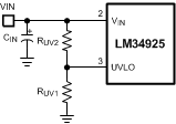
The LM34925 device contains a dual level Undervoltage Lockout (UVLO) circuit. A summary of threshold voltages and operational states is provided in the Device Functional Modes section. When the UVLO pin voltage is below 0.66 V, the controller is in a low current shutdown mode. When the UVLO pin voltage is greater than 0.66 V but less than 1.225 V, the controller is in standby mode. In standby mode the VCC bias regulator is active while the regulator output is disabled. When the VCC pin exceeds the VCC undervoltage thresholds and the UVLO pin voltage is greater than 1.225 V, normal operation begins. An external set-point voltage divider from VIN to GND can be used to set the minimum operating voltage of the regulator.
UVLO hysteresis is accomplished with an internal 20-μA current source that is switched on or off into the impedance of the set-point divider. When the UVLO threshold is exceeded, the current source is activated to quickly raise the voltage at the UVLO pin. The hysteresis is equal to the value of this current times the resistance RUV2.
If the UVLO pin is wired directly to the VIN pin, the regulator will begin operation once the VCC undervoltage is satisfied.
 Figure 10. UVLO Resistor Setting