ZHCSIQ5A September 2018 – August 2021 LM34936
PRODUCTION DATA
- 1 特性
- 2 应用
- 3 说明
- 4 Revision History
- 5 Pin Configuration and Functions
- 6 Specifications
-
7 Detailed Description
- 7.1 Overview
- 7.2 Functional Block Diagram
- 7.3
Feature Description
- 7.3.1 Fixed Frequency Valley/Peak Current Mode Control with Slope Compensation
- 7.3.2 VCC Regulator and Optional BIAS Input
- 7.3.3 Enable/UVLO
- 7.3.4 Soft-Start
- 7.3.5 Overcurrent Protection
- 7.3.6 Average Input/Output Current Limiting
- 7.3.7 Operation Above 28-V Input
- 7.3.8 CCM Operation
- 7.3.9 Frequency and Synchronization (RT/SYNC)
- 7.3.10 Frequency Dithering
- 7.3.11 Output Overvoltage Protection (OVP)
- 7.3.12 Power Good (PGOOD)
- 7.3.13 Gm Error Amplifier
- 7.3.14 Integrated Gate Drivers
- 7.3.15 Thermal Shutdown
- 7.4 Device Functional Modes
-
8 Application and Implementation
- 8.1 Application Information
- 8.2
Typical Application
- 8.2.1 Design Requirements
- 8.2.2
Detailed Design Procedure
- 8.2.2.1 Custom Design with WEBENCH Tools
- 8.2.2.2 Frequency
- 8.2.2.3 VOUT
- 8.2.2.4 Inductor Selection
- 8.2.2.5 Output Capacitor
- 8.2.2.6 Input Capacitor
- 8.2.2.7 Sense Resistor (RSENSE)
- 8.2.2.8 Slope Compensation
- 8.2.2.9 UVLO
- 8.2.2.10 Soft-Start Capacitor
- 8.2.2.11 Dither Capacitor
- 8.2.2.12 MOSFETs QH1 and QL1
- 8.2.2.13 MOSFETs QH2 and QL2
- 8.2.2.14 Frequency Compensation
- 8.2.3 Application Curves
- 9 Power Supply Recommendations
- 10Layout
- 11Device and Documentation Support
- 12Mechanical, Packaging, and Orderable Information
7.3.2 VCC Regulator and Optional BIAS Input
The VCC regulator provides a regulated bias supply to the gate drivers. When EN/UVLO is above the standby threshold (VEN(STBY)), the VCC regulator is turned on. For VIN less than the VCC regulation target, the VCC voltage tracks VIN with a small voltage drop as shown in Figure 6-4. If the EN/UVLO input is above the operating threshold (VEN(OP)) and VCC exceeds the VCC UV threshold (VUV(VCC)), the controller is enabled and switching begins.
The VCC regulator draws power from VIN when there is no supply voltage connected to the BIAS pin. If the BIAS pin is connected to an external voltage source that exceeds VCC by one diode drop, the VCC regulator draws power from the BIAS input instead of VIN. Connecting the BIAS pin to VOUT in applications with VOUT greater than 8.5 V improves the efficiency of the regulator in the buck mode.
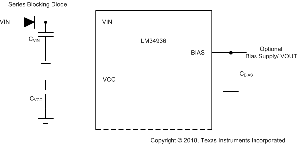
For low VIN operation, ensure that the VCC voltage is sufficient to fully enhance the MOSFETs. Use an external bias supply if VIN dips below the voltage required to sustain the VCC voltage. For these conditions, use a series blocking diode between the input supply and the VIN pin (Figure 7-1). This prevents VCC from back-feeding into VIN through the body diode of the VCC regulator.
A ceramic capacitor of 16 V or higher voltage rating and a value between 1 µF and 4.7 µF is required to supply the VCC regulator load transients. The VCC bypass capacitor should be connected between VCC and PGND pins.
 Figure 7-1 VCC Regulator and Optional BIAS