SNVS569C May 2009 – October 2016 LM3550
PRODUCTION DATA.
- 1 Features
- 2 Applications
- 3 Description
- 4 Revision History
- 5 Pin Configuration and Functions
- 6 Specifications
-
7 Detailed Description
- 7.1 Overview
- 7.2 Functional Block Diagram
- 7.3 Feature Description
- 7.4 Device Functional Modes
- 7.5 Programming
- 7.6 Register Maps
- 8 Application and Implementation
- 9 Power Supply Recommendations
- 10Layout
- 11Device and Documentation Support
- 12Mechanical, Packaging, and Orderable Information
8 Application and Implementation
NOTE
Information in the following applications sections is not part of the TI component specification, and TI does not warrant its accuracy or completeness. TI’s customers are responsible for determining suitability of components for their purposes. Customers should validate and test their design implementation to confirm system functionality.
8.1 Application Information
The LM3550 can drive multiple flash LEDs at currents up to 5 A total. The switched-capacitor boost on the LM3550 eliminates the need of an inductor in the application.
8.2 Typical Application
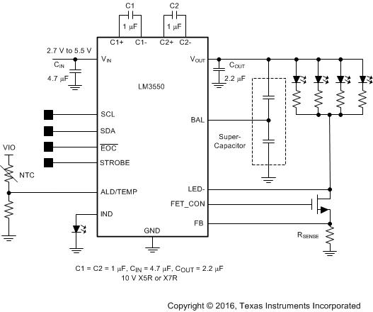 Figure 49. LM3550 Typical Application
8.2.1 Design Requirements
For LM3550, use the parameters listed in Table 10.
Table 10. Design Parameters
| DESIGN PARAMETER | EXAMPLE VALUE |
|---|---|
| Input voltage | 2.7 V to 5.5 V |
| Output voltage | 5.3 V (maximum) |
| Torch current | 0 to 200 mA (maximum) |
8.2.2 Detailed Design Procedure
8.2.2.1 Component Selection
8.2.2.1.1 Super-Capacitor
Super-capacitors, or electrochemical double-layer capacitors (EDLC's), have a very high energy density compared to other capacitor types. Most super-capacitors aimed at applications requiring voltages higher than 3V are three-terminal devices (two super-capacitor cells stacked in series). Special care must be taken to ensure that the voltage on each cell of the super-capacitor does not exceed the maximum rating (typically 2.75 V to
2.85 V, depending on the manufacturer). The LM3550 is capable of safely charging super-capacitors of many different capacitances up to a VOUT(maximum) = 5.3 V typical.
The capacitor balance pin (BAL) on the LM3550 ensures that the voltage on each cell is equal to half of the output voltage to prevent an overvoltage condition on either cell. If either cell fails as a short, the BAL pin does not prevent the second cell from being damaged.
NOTE
The LM3550 is not designed to work with low-voltage, single-cell super-capacitors.
8.2.2.1.2 Boost Capacitors
The LM3550 requires 4 external capacitors for proper operation (C1 = C2 = 1 µF; CIN = 4.7 µF; COUT = 2.2 µF); TI recommends surface-mount multi-layer ceramic capacitors are recommended. These capacitors are small, inexpensive and have very low equivalent series resistance (ESR < 20 mΩ typical). Tantalum capacitors, OS-CON capacitors, and aluminum electrolytic capacitors are not recommended for use with the LM3550 due to their high ESR, as compared to ceramic capacitors.
For most applications, ceramic capacitors with X7R or X5R temperature characteristic are preferred for use with the LM3550. These capacitors have tight capacitance tolerance (as good as ±10%) and hold their value over temperature (X7R: ±15% over −55°C to +125°C; X5R: ±15% over −55°C to +85°C).
Capacitors with Y5V or Z5U temperature characteristic are generally not recommended for use with the LM3550. Capacitors with these temperature characteristics typically have wide capacitance tolerance (+80%, −20%) and vary significantly over temperature (Y5V: 22%, −82% over −30°C to +85°C range; Z5U: 22%, −56% over 10°C to 85°C range). Under some conditions, a nominal 1µF Y5V or Z5U capacitor could have a capacitance of only 0.1 µF. Such detrimental deviation is likely to cause Y5V and Z5U capacitors to fail to meet the minimum capacitance requirements of the LM3550.
The recommended voltage rating for the capacitors is 10 V to account for DC bias capacitance losses.
8.2.2.1.3 Current Source FET
Choose the proper current source MOSFET to ensure accurate flash current delivery. N-channel MOSFETs (NFET) with allowed drain-to-source voltages (VDS) greater than 5.5 V are required. In order to prevent damage to the current source NFET, special attention must be given to the pulsed-current rating of the MOSFET. The NFET must be sized appropriately to handle the desired flash current and flash duration. Most MOSFET manufacturers provide curves showing the pulsed performance of the NFET in the electrical characteristics section of their data sheets. The performance of the MOSFET rating at temperature, primarily temperatures greater than 40°C, must also be investigated to ensure NFET does not become thermally damaged during a flash pulse. An NFET possessing low RDSON values helps improve the efficiency of the flash pulse.
8.2.2.1.4 ALD/TEMP Components
8.2.2.1.4.1 NTC Selection
NTC thermistors have a temperature-to-resistance relationship of:

where
- β is given in the thermistor data sheet
- R25°C is the thermistor's value at 25°C
R1 in is chosen so that it is equal to:

where
- RT(TRIP) is the thermistors value at the temperature trip point
- VBIAS is shown in Figure 50
- VTRIP = 800 mV (typical)
Choosing R1 here gives a more linear response around the temperature trip voltage. For example, with VBIAS = 1.8 V, a thermistor whose nominal value at 25°C is 100 kΩ, and a β = 4500 K, the trip point is chosen to be 85°C. The value of R(T) at 85°C is:

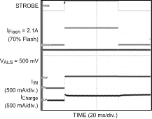
Setting the ALD/TEMP Sense High Register to N = 50 or hex 0x32 places the upper trip point to approximately 800 mV. Voltages higher than 800 mV prevent the flash LED from turning on. Based on Figure 50, the Sense Low Register can be set to a lower code to give a second LED current threshold (70% flash). Voltages lower than the value stored in the Sense Low Register allow a full current flash.
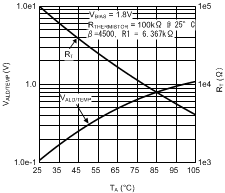 Figure 50. Thermistor Resistive Divider Response vs Temperature
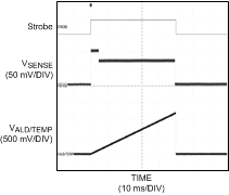
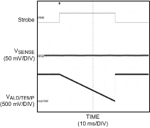
If the temperature changes during a flash event, meaning VALS/TEMP crosses the sense high and/or sense low values, the current scales to the appropriate zone current.
Place the thermistor as close as possible to the flash LEDs. This provides the best thermal coupling (lowest thermal resistance).
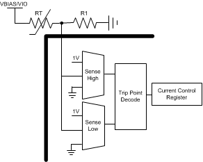 Figure 51. Thermistor Voltage Divider and Sensing Circuit
8.2.2.1.4.2 Ambient Light Sensor
If the ALD/TEMP pin is not used for ambient/LED temperature monitoring, it can be used for ambient light detection. The LM3550 provides three regions of current control based upon ambient conditions. The three regions are defined using the Sense High and Sense Low Registers to set the zone boundaries (user-configurable from 0 to 1 V). Most ambient light sensors are reverse-biased diodes that leak current proportional to the amount of ambient light reaching the sensor. This current is then translated into a voltage by using a resistor in series with the light sensor. The voltage-setting resistor varies based upon the desired ambient detection range and manufacturer.
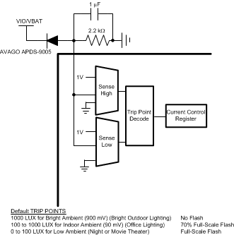
Most ambient light sensors suggest placing a capacitor in parallel with the voltage-setting resistor in order to help filter the 50-, 60-Hz noise generated by fluorescent overhead lighting. This capacitor can range from no capacitor up to 10 µF. The key is to filter the noise so that the peak-to-peak voltage is less than 16 mV (LSB size of the ALD/TEMP sense high and sense low settings). Refer to the data sheet of the ambient light sensor for the recommended capacitor value.
8.2.2.1.5 Thermal Protection
Internal thermal protection circuitry disables the LM3550 when the junction temperature exceeds 145°C (typical). This feature protects the device from being damaged by high die temperatures that might otherwise result from excessive power dissipation. The device recovers and operates normally when the junction temperature falls below 125°C (typical). It is important that the board layout provide good thermal conduction to keep the junction temperature within the specified operating ratings.
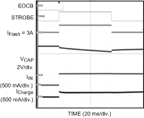
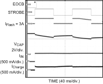
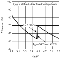
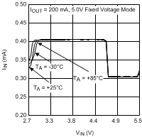
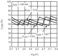
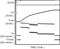
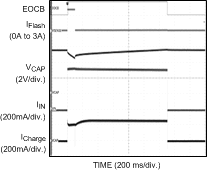
8.2.3 Application Curves
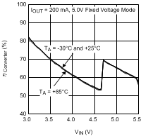
| 5-V Mode |
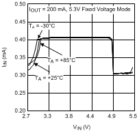
| 5.3-V Mode |
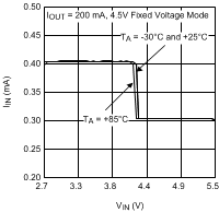
| 4.5-V Mode |
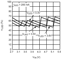
| 200 mA |
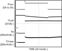
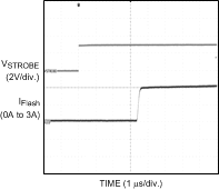
| VALS = 500 mV |
| 4.5-V Mode |
| 5-V Mode |
| 100 mA |
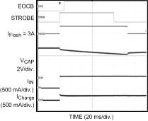
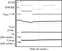
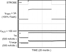
| VALS = 100 mV |
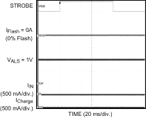
| VALS = 1 V |