SNVSCV4 September 2024 LM3645
PRODUCTION DATA
- 1
- 1 Features
- 2 Applications
- 3 Description
- 4 Pin Configuration and Functions
- 5 Specifications
-
6 Detailed Description
- 6.1 Overview
- 6.2 Functional Block Diagram
- 6.3
Feature Description
- 6.3.1 Power Amplifier Synchronization (TORCH/TX)
- 6.3.2 Input Voltage Flash Monitor (IVFM)
- 6.3.3
Fault/Protections
- 6.3.3.1 Fault Operation
- 6.3.3.2 Flash Time-Out
- 6.3.3.3 Overvoltage Protection (OVP)
- 6.3.3.4 Current Limit
- 6.3.3.5 NTC Thermistor Input/Outputs (TEMP1, TEMP2)
- 6.3.3.6 Thermal Scale Back
- 6.3.3.7 Thermal Shutdown (TSD)
- 6.3.3.8 Undervoltage Lockout (UVLO)
- 6.3.3.9 LED and/or VOUT Short Fault
- 6.3.3.10 Fault Behavior Table
- 6.4 Device Functioning Modes
- 6.5 Programming and Control
- 6.6 Register Descriptions
- 7 Application and Implementation
- 8 Power Supply Recommendations
- 9 Layout
- 10Device and Documentation Support
- 11Revision History
- 12Mechanical, Packaging, and Orderable Information
6.3.3.5 NTC Thermistor Input/Outputs (TEMP1, TEMP2)
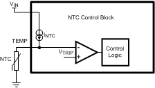
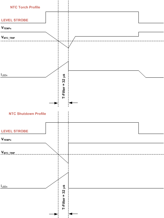
The TEMP1 and TEMP2 pins serve as a threshold detector and bias source for negative temperature coefficient (NTC) thermistors. When the voltage at TEMPx goes below the programmed threshold, the LM3645 device transitions into one of these three modes:
- Force standby mode
- Force torch mode
- Report only mode (bits [5:2] in reg 0x0D)
The device allows adjustment of the NTC threshold voltage from 250 mV to 1 V in 50 mV steps (bits [7:0] in reg 0x0F). Additionally, the NTC1 and NTC2 voltage levels provide an indicator of the remotely sensed temperature. The NTC bias current is adjustable in 25 µA steps from 25 µA to 100 µA (bits [7:6] in reg 0x0D). The NTC1 and NTC2 detection circuitry can be enabled or disabled via the NTC_MODE Register (bits [1:0] in reg 0x0D). If enabled, the NTC block turns on and off during the start and stop of a Flash/Torch/IR event.
Additionally, the NTC input looks for an open NTC connection and a shorted NTC connection. If the NTC input falls below 100 mV, the NTC short flag is set, and the device is disabled (bits [7:6] in reg 0x16). If the NTC input rises above 2.0 V, the NTC Open flag is set, and the device is disabled (bits [5:4] in reg 0x16). These fault detections can be individually disabled or enabled via the NTC Open Fault Enable bit (bits [2] in reg 0x13) and the NTC Short Fault Enable bit (bit [0] in reg 0x13).
 Figure 6-3 Temp Detection Diagram
To further extend the functionality of the NTC inputs, the voltage on both TEMP1 and TEMP2 can be read back to provide real time feedback regarding the temperature at the point of detection (bits [7:0] in reg 0x10). When either TEMP1 or TEMP2 pin is enabled, a 4-bit ADC is enabled and continually updates the NTC Voltage Register. The voltage on both TEMP1 and TEMP2 are measured if either NTC detection block is enabled. In this case, the data read into the NTC voltage register for the disabled TEMP detection block can be random and can be ignored. Only enabled TEMP blocks yield accurate readings.
Each NTC block can be associated with any of the four outputs. Each Dx Output should only be assigned to one of the NTC detection blocks.
 Figure 6-4 NTC Detection Diagram