SNVSCV4 September   2024 LM3645

PRODUCTION DATA  

  1.   1
  2. Features
  3. Applications
  4. Description
  5. Pin Configuration and Functions
  6. Specifications
    1. 5.1 Absolute Maximum Ratings
    2. 5.2 ESD Ratings
    3. 5.3 Recommended Operating Conditions
    4. 5.4 Thermal Information
    5. 5.5 Electrical Characteristics
    6. 5.6 Timing Requirements
    7. 5.7 Switching Characteristics
    8. 5.8 Typical Characteristics
  7. Detailed Description
    1. 6.1 Overview
    2. 6.2 Functional Block Diagram
    3. 6.3 Feature Description
      1. 6.3.1 Power Amplifier Synchronization (TORCH/TX)
      2. 6.3.2 Input Voltage Flash Monitor (IVFM)
      3. 6.3.3 Fault/Protections
        1. 6.3.3.1  Fault Operation
        2. 6.3.3.2  Flash Time-Out
        3. 6.3.3.3  Overvoltage Protection (OVP)
        4. 6.3.3.4  Current Limit
        5. 6.3.3.5  NTC Thermistor Input/Outputs (TEMP1, TEMP2)
        6. 6.3.3.6  Thermal Scale Back
        7. 6.3.3.7  Thermal Shutdown (TSD)
        8. 6.3.3.8  Undervoltage Lockout (UVLO)
        9. 6.3.3.9  LED and/or VOUT Short Fault
        10. 6.3.3.10 Fault Behavior Table
    4. 6.4 Device Functioning Modes
      1. 6.4.1 Flash Mode
      2. 6.4.2 Torch Mode
      3. 6.4.3 IR Mode
      4. 6.4.4 Voltage Mode
      5. 6.4.5 Mode Transitions
      6. 6.4.6 Boost Operation
        1. 6.4.6.1 Start-Up (Enabling The Device)
        2. 6.4.6.2 Pass Mode
        3. 6.4.6.3 Output Voltage Regulation
    5. 6.5 Programming and Control
      1. 6.5.1 Dx_EN Bits
      2. 6.5.2 STR1 and STR2 Usage
      3. 6.5.3 TOR/TX Usage
      4. 6.5.4 Control State Diagram
      5. 6.5.5 I2C-Compatible Interface
        1. 6.5.5.1 Data Validity
        2. 6.5.5.2 Start and Stop Conditions
        3. 6.5.5.3 Transferring Data
        4. 6.5.5.4 I2C-Compatible Chip Address
    6. 6.6 Register Descriptions
      1. 6.6.1 MainReg Registers
  8. Application and Implementation
    1. 7.1 Application Information
    2. 7.2 Typical Application
      1. 7.2.1 Design Requirements
      2. 7.2.2 Output Control Examples
        1. 7.2.2.1 Four Channel Flash with Strobe1 Trigger Starting in Standby
        2. 7.2.2.2 Four Channel Flash with Strobe1 Trigger Starting in I2C Torch
        3. 7.2.2.3 Mixed Mode Functionality
        4. 7.2.2.4 Voltage Mode Only
        5. 7.2.2.5 Voltage Mode With Advanced IR
      3. 7.2.3 Detailed Design Procedure
        1. 7.2.3.1 Snubber Requirement
        2. 7.2.3.2 Output Capacitor Selection
        3. 7.2.3.3 Input Capacitor Selection
        4. 7.2.3.4 Inductor Selection
      4. 7.2.4 Application Curves
  9. Power Supply Recommendations
  10. Layout
    1. 9.1 Layout Guidelines
    2. 9.2 Layout Example
  11. 10Device and Documentation Support
    1. 10.1 Third-Party Products Disclaimer
    2. 10.2 Receiving Notification of Documentation Updates
    3. 10.3 Support Resources
    4. 10.4 Trademarks
    5. 10.5 Electrostatic Discharge Caution
    6. 10.6 Glossary
  12. 11Revision History
  13. 12Mechanical, Packaging, and Orderable Information

封装选项

机械数据 (封装 | 引脚)
散热焊盘机械数据 (封装 | 引脚)
订购信息

IR Mode

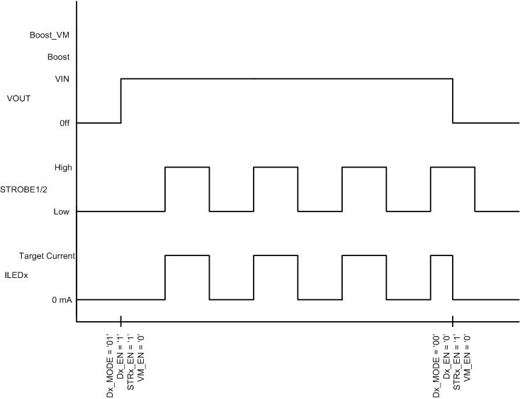
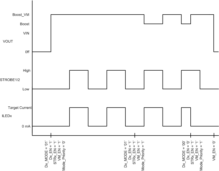
In IR Mode, the target LED current is equal to the value stored in the LED1/2/3/4 Flash Brightness Registers. When IR mode is enabled on any of the outputs, the boost converter turns on and set the output equal to the input (pass-mode) or to the selected voltage mode depending upon the state of the voltage mode settings. At this point, toggling the STROBE pins enables and disables the LED1/2/3/4 current sources (if enabled via the Dx Mode bits). The strobe pins can only be set to be Level sensitive, meaning all timing of the IR pulse is externally controlled. If the strobe pin is set to edge mode, the LM3645 device times out after the end of the set duration. In IR Mode, the current sources either ramp quickly or do not ramp the LED outputs to the target based upon the ramp time setting chosen.
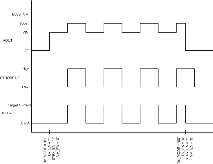
LM3645 IR Mode with BoostFigure 6-6 IR Mode with Boost
LM3645 IR Mode Pass OnlyFigure 6-7 IR Mode Pass Only
LM3645 IR Mode Voltage Mode EnabledFigure 6-8 IR Mode Voltage Mode Enabled