SNVS405G December 2005 – April 2015 LM3674
PRODUCTION DATA.
- 1 Features
- 2 Applications
- 3 Description
- 4 Revision History
- 5 Pin Configuration and Functions
- 6 Specifications
- 7 Detailed Description
- 8 Application and Implementation
- 9 Power Supply Recommendations
- 10Layout
- 11Device and Documentation Support
- 12Mechanical, Packaging, and Orderable Information
10 Layout
10.1 Layout Guidelines
PC board layout is an important part of DC-DC converter design. Poor board layout can disrupt the performance of a DC-DC converter and surrounding circuitry by contributing to EMI, ground bounce, and resistive voltage loss in the traces. These can send erroneous signals to the DC-DC converter device, resulting in poor regulation or instability.
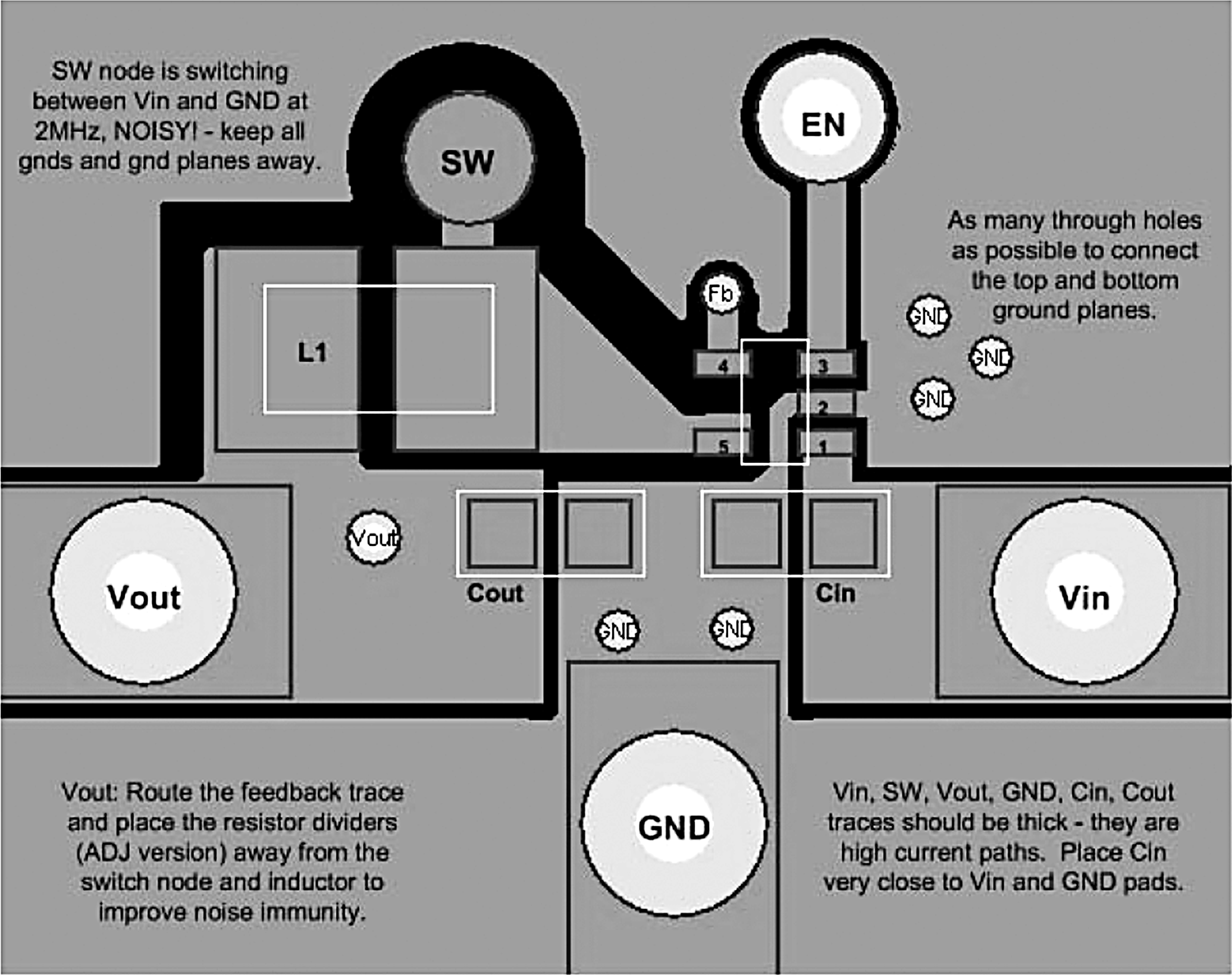
Good layout for the LM3674 can be implemented by following a few simple design rules, as illustrated in Figure 21.
- Place the LM3674, inductor and filter capacitors close together and make the traces short. The traces between these components carry relatively high switching currents and act as antennas. Following this rule reduces radiated noise. Special care must by given to place the input filter capacitor very close to the VIN and GND pin.
- Arrange the components so that the switching current loops curl in the same direction. During the first half of each cycle, current flows from the input filter capacitor, through the LM3674 and inductor to the output filter capacitor and back through ground, forming a current loop. In the second half of each cycle, current is pulled up from ground, through the LM3674 by the inductor, to the output filter capacitor and then back through ground, forming a second current loop. Routing these loops so the current curls in the same direction prevents magnetic field reversal between the two half-cycles and reduces radiated noise.
- Connect the ground pins of the LM3674, and filter capacitors together using generous component-side copper fill as a pseudo-ground plane. Then, connect this to the ground-plane (if one is used) with several vias. This reduces ground-plane noise by preventing the switching currents from circulating through the ground plane. It also reduces ground bounce at the LM3674 by giving it a low-impedance ground connection.
- Use wide traces between the power components and for power connections to the DC-DC converter circuit. This reduces voltage errors caused by resistive losses across the traces.
- Route noise sensitive traces, such as the voltage feedback path, away from noisy traces between the power components. The voltage feedback trace must remain close to the LM3674 circuit and should be direct but should be routed opposite to noisy components. This reduces the EMI radiated onto the voltage feedback trace of the DC-DC converter. A good approach is to route the feedback trace on another layer and to have a ground plane between the top layer and layer on which the feedback trace is routed. In the same manner for the adjustable part it is desired to have the feedback dividers on the bottom layer.
- Place noise sensitive circuitry, such as radio IF blocks, away from the DC-DC converter, CMOS digital blocks and other noisy circuitry. Interference with noise-sensitive circuitry in the system can be reduced through distance.
In mobile phones, for example, a common practice is to place the DC-DC converter on one corner of the board, arrange the CMOS digital circuitry around it (because this also generates noise), and then place sensitive preamplifiers and IF stages on the diagonally opposing corner. Often, the sensitive circuitry is shielded with a metal pan and power to it is post-regulated to reduce conducted noise by using low-dropout linear regulators.
10.2 Layout Example
 Figure 21. Board Layout Design Rules for the LM3674