SNVS405G December   2005  – April 2015 LM3674

PRODUCTION DATA.  

  1. Features
  2. Applications
  3. Description
  4. Revision History
  5. Pin Configuration and Functions
  6. Specifications
    1. 6.1 Absolute Maximum Ratings
    2. 6.2 ESD Ratings
    3. 6.3 Recommended Operating Conditions
    4. 6.4 Thermal Information
    5. 6.5 Dissipation Ratings
    6. 6.6 Electrical Characteristics
    7. 6.7 Typical Characteristics
  7. Detailed Description
    1. 7.1 Overview
    2. 7.2 Functional Block Diagram
    3. 7.3 Feature Description
      1. 7.3.1 Circuit Operation
      2. 7.3.2 PWM Operation
        1. 7.3.2.1 Internal Synchronous Rectification
        2. 7.3.2.2 Current Limiting
    4. 7.4 Device Functional Modes
  8. Application and Implementation
    1. 8.1 Application Information
      1. 8.1.1 Soft-Start
      2. 8.1.2 Low-Dropout (LDO) Operation
    2. 8.2 Typical Applications
      1. 8.2.1 Typical Application for Fixed Voltage Configuration
        1. 8.2.1.1 Design Requirements
        2. 8.2.1.2 Detailed Design Procedure
          1. 8.2.1.2.1 Inductor Selection
          2. 8.2.1.2.2 Input Capacitor Selection
          3. 8.2.1.2.3 Output Capacitor Selection
        3. 8.2.1.3 Application Curves
      2. 8.2.2 Typical Application Circuit for Adjustable Voltage Option
        1. 8.2.2.1 Design Requirements
        2. 8.2.2.2 Detailed Design Procedure
          1. 8.2.2.2.1 Output Voltage Selection for Adjustable (LM3674-ADJ)
        3. 8.2.2.3 Application Curves
  9. Power Supply Recommendations
  10. 10Layout
    1. 10.1 Layout Guidelines
    2. 10.2 Layout Example
  11. 11Device and Documentation Support
    1. 11.1 Device Support
      1. 11.1.1 Third-Party Products Disclaimer
    2. 11.2 Trademarks
    3. 11.3 Electrostatic Discharge Caution
    4. 11.4 Glossary
  12. 12Mechanical, Packaging, and Orderable Information

封装选项

机械数据 (封装 | 引脚)
散热焊盘机械数据 (封装 | 引脚)
订购信息

5 Pin Configuration and Functions

DBV Package
5-Pin SOT-23
Top View
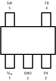
LM3674 20167202.gif
Note: The actual physical placement of the package marking will vary from part to part.

Pin Functions

PIN TYPE DESCRIPTION
NAME NUMBER
EN 3 Digital Enable input. The device is in shutdown mode when voltage to this pin is < 0.4 V and enable when > 1 V. Do not leave this pin floating.
FB 4 Analog Feedback analog input. Connect to the output filter capacitor, COUT, for fixed voltage versions. For adjustable version, external resistor dividers are required (R1 and R2). The internal resistor dividers are disabled for the adjustable version.
GND 2 Ground Ground pin
SW 5 Analog Switching node connection to the internal PFET switch and NFET synchronous rectifier.
VIN 1 Power Power supply input. Connect to the input filter capacitor, CIN.