SNVS405G December 2005 – April 2015 LM3674
PRODUCTION DATA.
- 1 Features
- 2 Applications
- 3 Description
- 4 Revision History
- 5 Pin Configuration and Functions
- 6 Specifications
- 7 Detailed Description
- 8 Application and Implementation
- 9 Power Supply Recommendations
- 10Layout
- 11Device and Documentation Support
- 12Mechanical, Packaging, and Orderable Information
6 Specifications
6.1 Absolute Maximum Ratings
over operating free-air temperature range (unless otherwise noted)(1)(2)| MIN | MAX | UNIT | |
|---|---|---|---|
| VIN pin: voltage to GND | −0.2 | 6 | V |
| EN, FB, and SW pins | GND − 0.2 | VIN + 0.2 | V |
| Continuous power dissipation(3) | Internally Limited | ||
| Junction temperature (TJ-MAX) | 125 | °C | |
| Maximum lead temperature (soldering, 10 seconds) | 260 | °C | |
| Storage temperature, Tstg | –65 | °C | |
(1) Stresses beyond those listed under Absolute Maximum Ratings may cause permanent damage to the device. These are stress ratings only, which do not imply functional operation of the device at these or any other conditions beyond those indicated under Recommended Operating Conditions. Exposure to absolute-maximum-rated conditions for extended periods may affect device reliability.
(2) If Military- or Aerospace-specified devices are required, please contact the TI Sales Office/Distributors for availability and specifications.
(3) In applications where high power dissipation and/or poor package resistance is present, the maximum ambient temperature may have to be derated. Maximum ambient temperature (TA-MAX) is dependent on the maximum operating junction temperature (TJ-MAX), the maximum power dissipation of the device in the application (PD-MAX) and the junction-to-ambient thermal resistance of the package (RθJA) in the application, as given by the following equation: TA-MAX = TJ-MAX – (RθJA × PD-MAX). See Dissipation Ratings for PD-MAX values at different ambient temperatures.
6.2 ESD Ratings
| VALUE | UNIT | |||
|---|---|---|---|---|
| V(ESD) | Electrostatic discharge | Human body model (HBM), per ANSI/ESDA/JEDEC JS-001, all pins(1) | ±2000 | V |
| Charged device model (CDM), per JEDEC specification JESD22-C101, all pins(2) | ±200 | V | ||
(1) JEDEC document JEP155 states that 500-V HBM allows safe manufacturing with a standard ESD control process.
(2) JEDEC document JEP157 states that 250-V CDM allows safe manufacturing with a standard ESD control process.
6.3 Recommended Operating Conditions
over operating free-air temperature range (unless otherwise noted)(1)| MIN | MAX | UNIT | |
|---|---|---|---|
| Input voltage(2) | 2.7 | 5.5 | V |
| Recommended load current | 0 | 600 | mA |
| Junction temperature, TJ | –30 | 125 | °C |
| Ambient temperature,TA | –30 | 85 | °C |
(1) All voltages are with respect to the potential at the GND pin.
(2) Input voltage range recommended for ideal applications performance for the specified output voltages are given below:
VIN = 2.7 V to 5.5 V for 1 V ≤ VOUT < 1.8 V
VIN = (VOUT + VDROP OUT) to 5.5 V for 1.8 ≤ VOUT ≤ 3.3 V, where VDROP OUT = ILOAD × (RDSON (P) + RINDUCTOR)
VIN = 2.7 V to 5.5 V for 1 V ≤ VOUT < 1.8 V
VIN = (VOUT + VDROP OUT) to 5.5 V for 1.8 ≤ VOUT ≤ 3.3 V, where VDROP OUT = ILOAD × (RDSON (P) + RINDUCTOR)
6.4 Thermal Information
| THERMAL METRIC(1) | LM3674 | UNIT | ||
|---|---|---|---|---|
| DBV (SOT-23) | ||||
| 5 PINS | ||||
| RθJA | Junction-to-ambient thermal resistance | 4-layer board | 130 | °C/W |
| 2-layer board | 250 | |||
(1) For more information about traditional and new thermal metrics, see the IC Package Thermal Metrics application report, SPRA953.
6.5 Dissipation Ratings
over operating free-air temperature range (unless otherwise noted)| RθJA | TA ≤ 25°C (POWER RATING) | TA = 60°C (POWER RATING) | TA = 85°C (POWER RATING) |
|---|---|---|---|
| 250°C/W (2-layer board) | 400 mW | 260 mW | 160 mW |
| 130°C/W (4-layer board) | 770 mW | 500 mW | 310 mW |
6.6 Electrical Characteristics
Typical limits are TA = 25°C; unless otherwise noted, specifications apply to the LM3674 with VIN = EN = 3.6 V(1)(2)(3)| PARAMETER | TEST CONDITIONS | MIN | TYP | MAX | UNIT | |
|---|---|---|---|---|---|---|
| VFB | Feedback voltage(4)(5) | IO = 10 mA, −30°C ≤ TJ ≤ 125°C | –4% | 4% | ||
| Line regulation | 2.7 V ≤ VIN ≤ 5.5 V, IO = 100 mA | 0.083 | %/V | |||
| Load regulation | 100 mA ≤ IO ≤ 600 mA, VIN = 3.6 V | 0.0010 | %/mA | |||
| VREF | Internal reference voltage | See(6) | 0.5 | V | ||
| ISHDN | Shutdown supply current | EN = 0 V | 0.01 | µA | ||
| EN = 0 V, –30°C ≤ TJ ≤ 125°C | 1 | |||||
| IQ | DC bias current into VIN | No load, device is not switching (FB = 0 V) | 300 | µA | ||
| No load, device is not switching (FB = 0 V) –30°C ≤ TJ ≤ 125°C |
600 | |||||
| RDSON (P) | Pin-to-pin resistance for PFET | ISW = 200 mA | 380 | 500 | mΩ | |
| RDSON (N) | Pin-to-pin resistance for NFET | ISW = 200 mA | 250 | 400 | mΩ | |
| ILIM | Switch peak current limit | Open loop(7) | 1020 | mA | ||
| Open loop(7), –30°C ≤ TJ ≤ 125°C | 830 | 1200 | ||||
| VIH | Logic high input | –30°C ≤ TJ ≤ 125°C | 1 | V | ||
| VIL | Logic low input | –30°C ≤ TJ ≤ 125°C | 0.4 | V | ||
| IEN | Enable (EN) input current | 0.01 | µA | |||
| –30°C ≤ TJ ≤ 125°C | 1 | |||||
| FOSC | Internal oscillator frequency | PWM mode | 2 | MHz | ||
| PWM mode, −30°C ≤ TJ ≤ 125°C | 1.6 | 2.6 | ||||
(1) All voltages are with respect to the potential at the GND pin.
(2) Minimum and maximum limits are specified by design, test, or statistical analysis. Typical numbers represent the most likely values.
(3) The parameters in the Electrical Characteristics are tested at VIN = 3.6 V unless otherwise specified. For performance curves over the input voltage range, see Typical Characteristics.
(4) ADJ configured to 1.5-V output.
(5) For VOUT < 2.5 V, VIN = 3.6 V; for VOUT ≥ 2.5 V, VIN = VOUT + 1.
(6) For the ADJ version the resistor dividers should be selected such that at the desired output voltage, the voltage at the FB pin is 0.5 V.
(7) See Typical Characteristics for closed loop data and its variation with regards to supply voltage and temperature. Electrical Characteristics reflect open loop data (FB = 0 V and current drawn from the SW pin ramped up until cycle-by-cycle current limit is activated). Closed-loop current limit is the peak inductor current measured in the application circuit by increasing output current until output voltage drops by 10%.
6.7 Typical Characteristics
(unless otherwise stated: VIN = 3.6 V, VOUT = 1.5 V, TA = 25°C)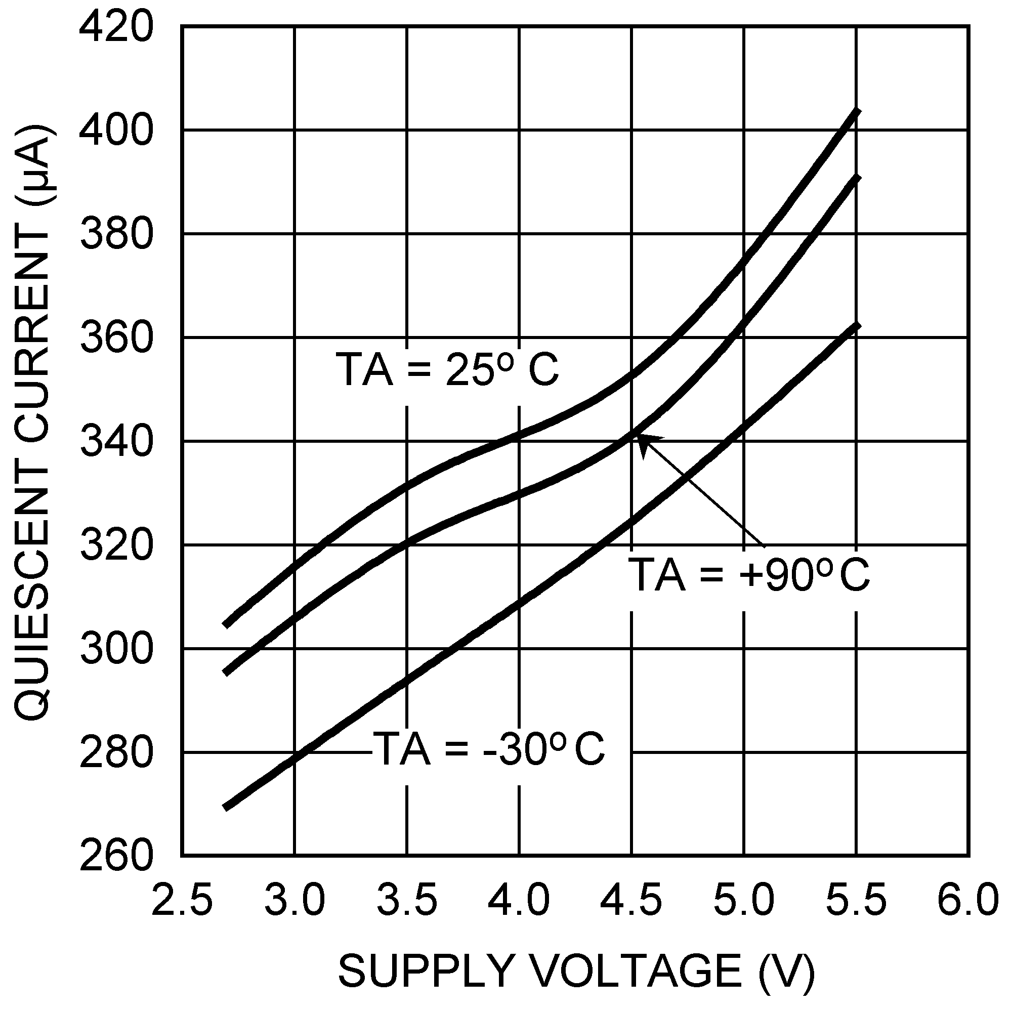
| FB = 0 V, No Switching |
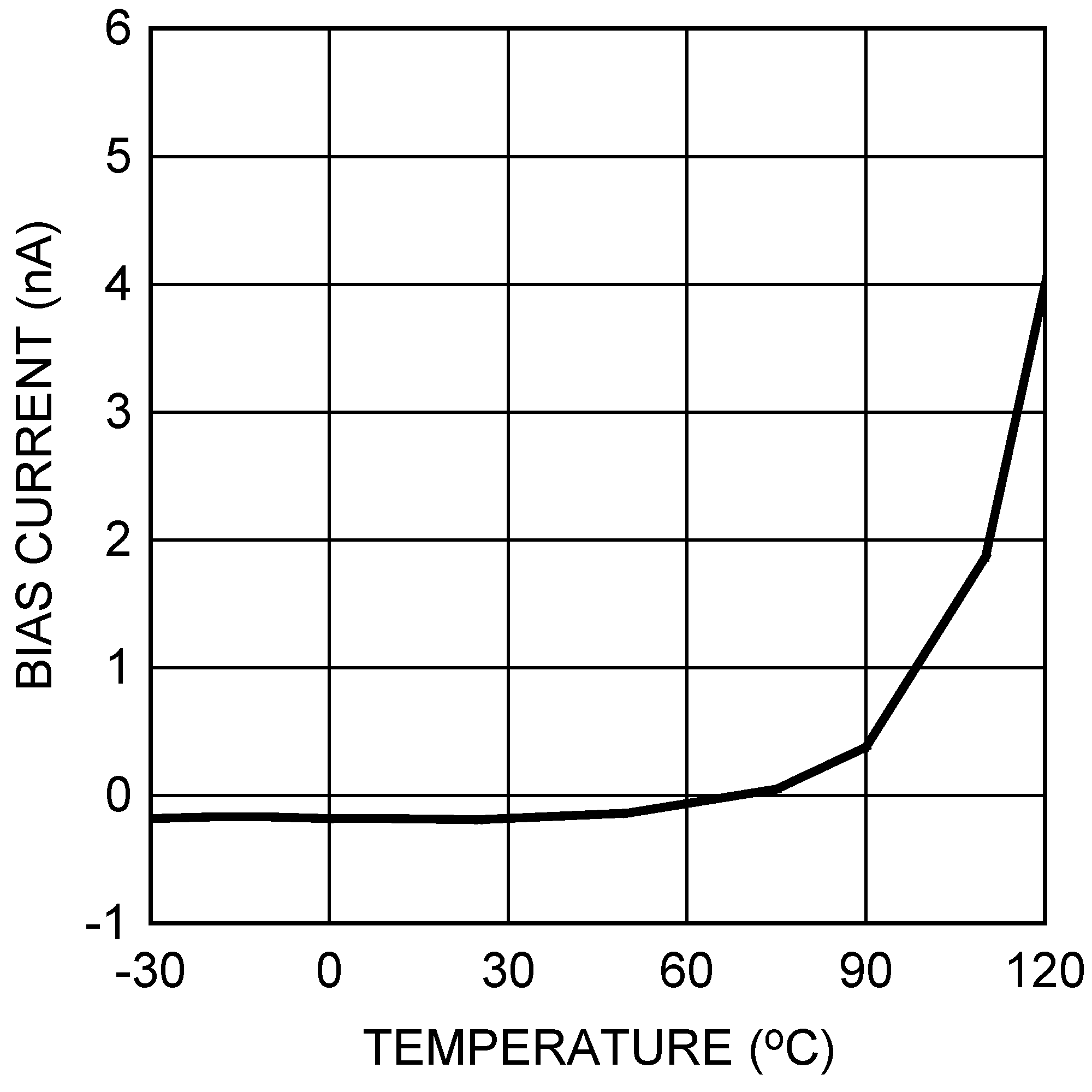 Figure 3. Feedback Bias Current vs Temperature
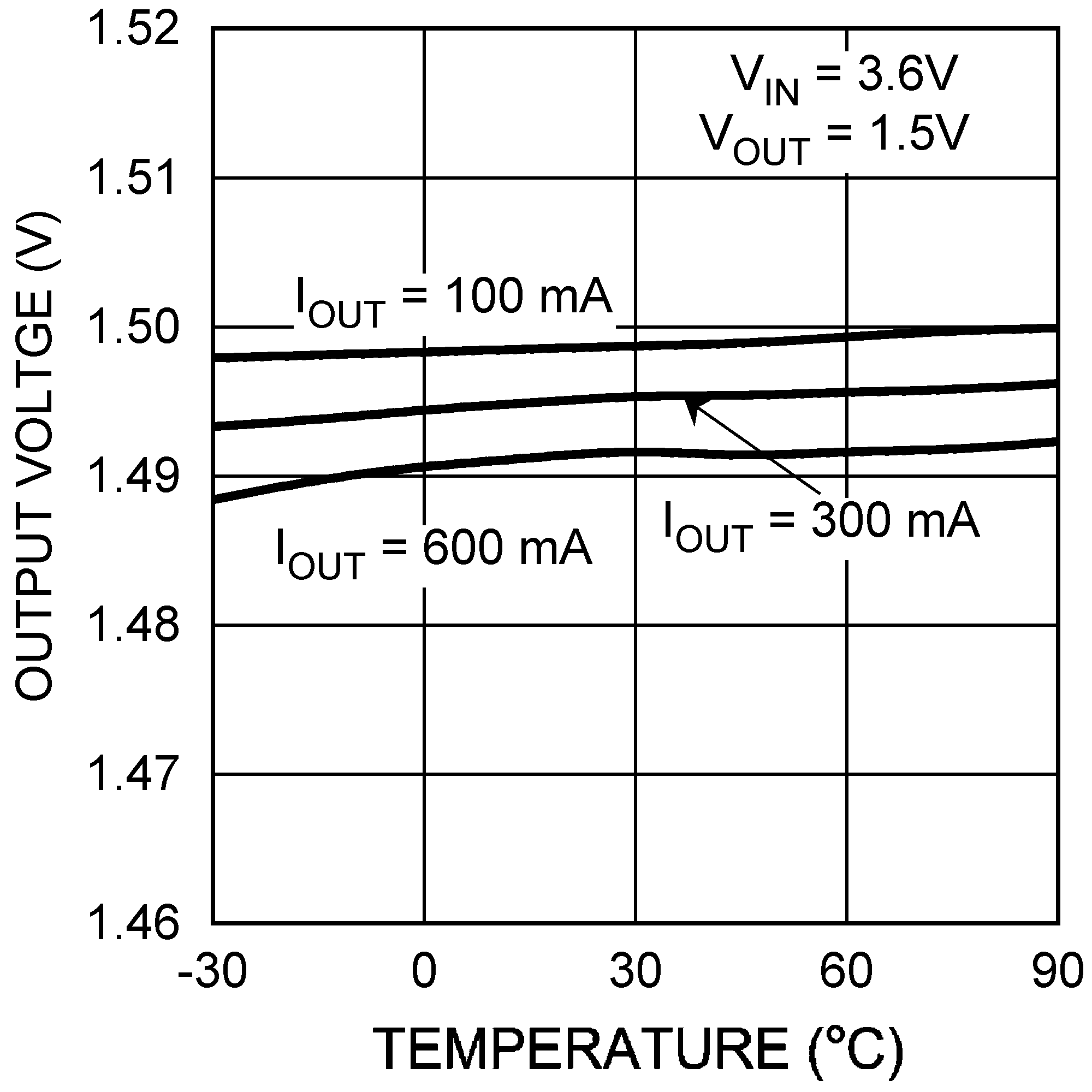 Figure 5. Output Voltage vs Temperature
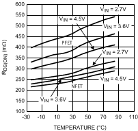 Figure 7. RDSON vs Temperature
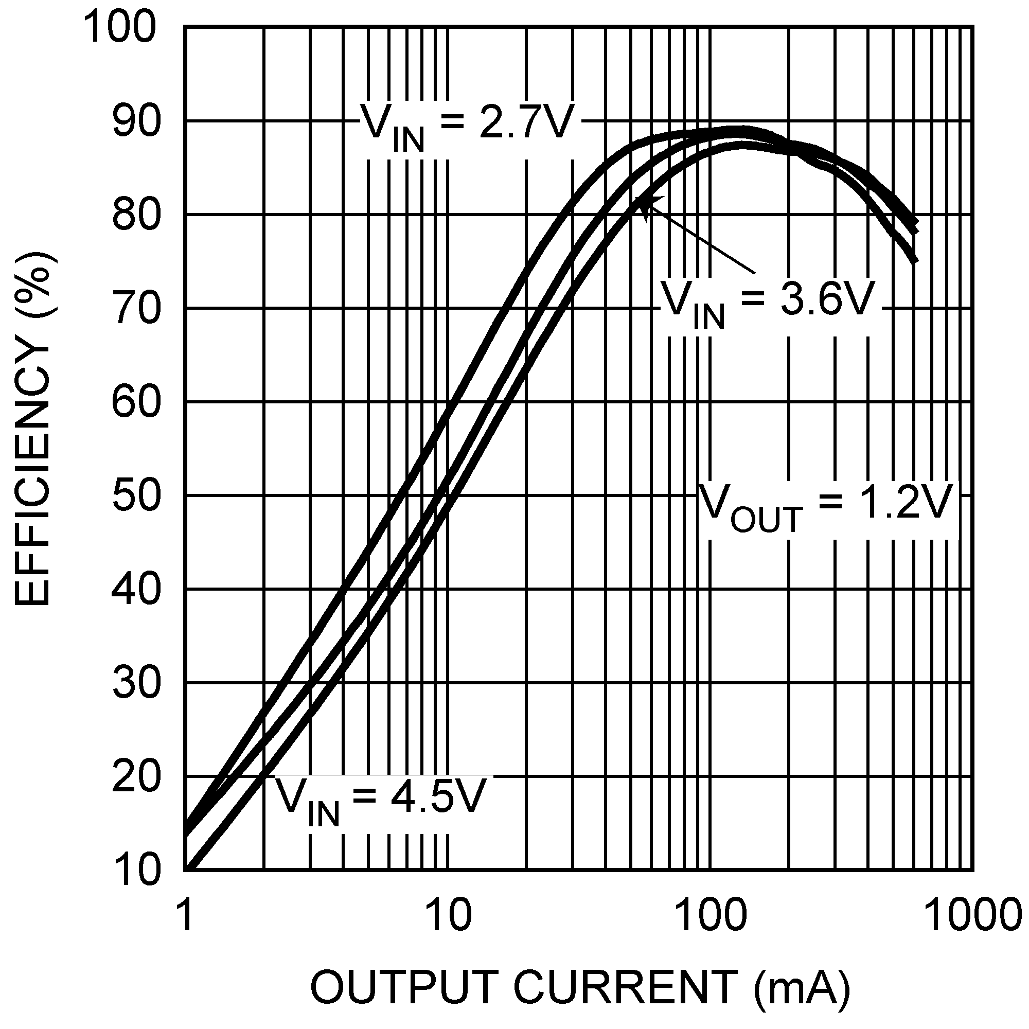
| VOUT = 1.2 V, L = 2.2 µH, DCR = 200 mΩ |
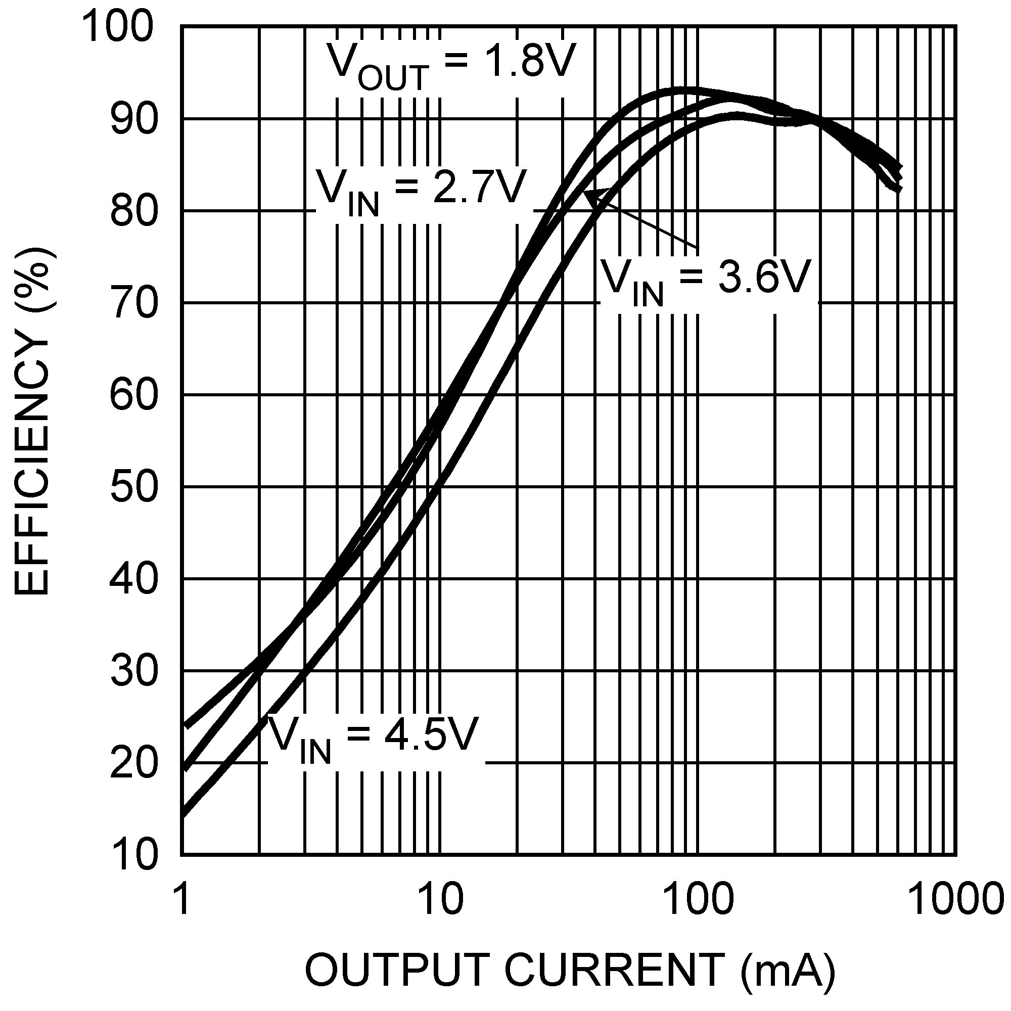
| VOUT = 1.8 V, L = 2.2 µH, DCR = 200 mΩ |
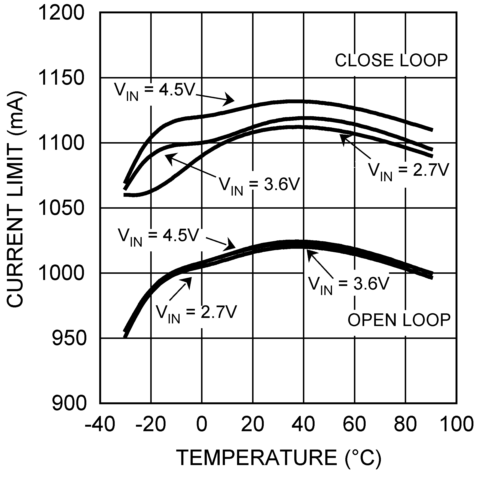
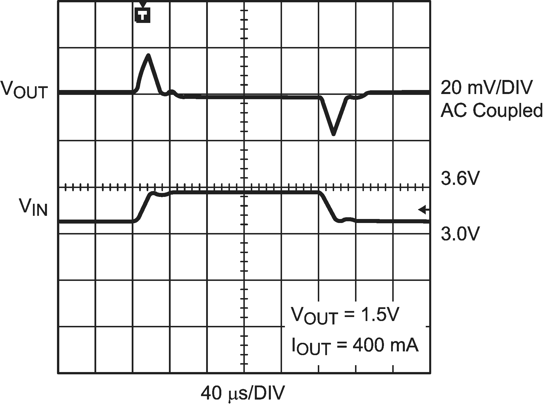
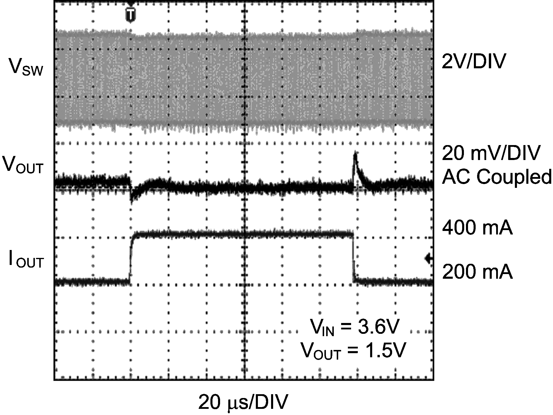 Figure 15. Load Transient
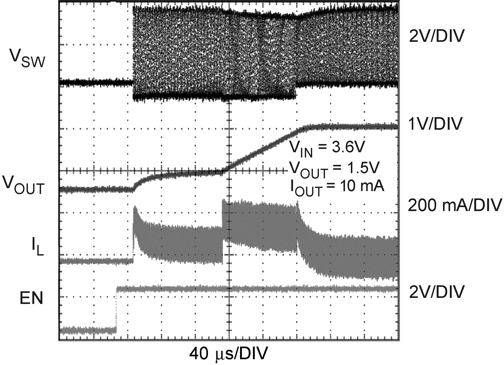
| Output Current = 10 mA |
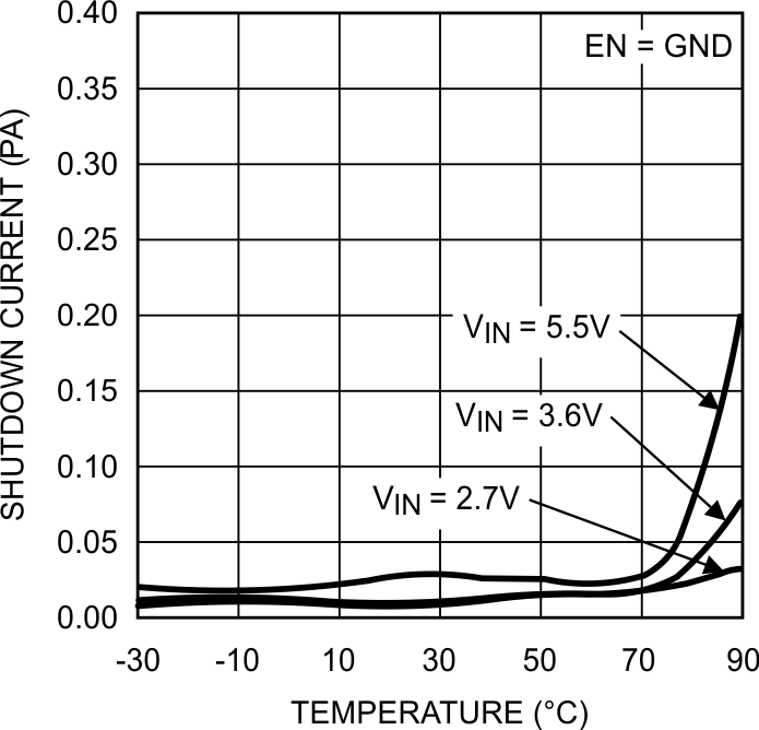 Figure 2. IQ Shutdown vs Temperature
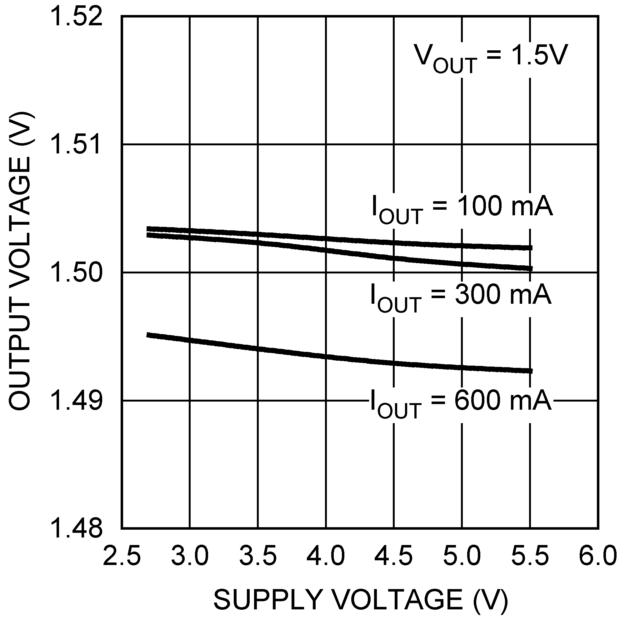 Figure 4. Output Voltage vs Supply Voltage
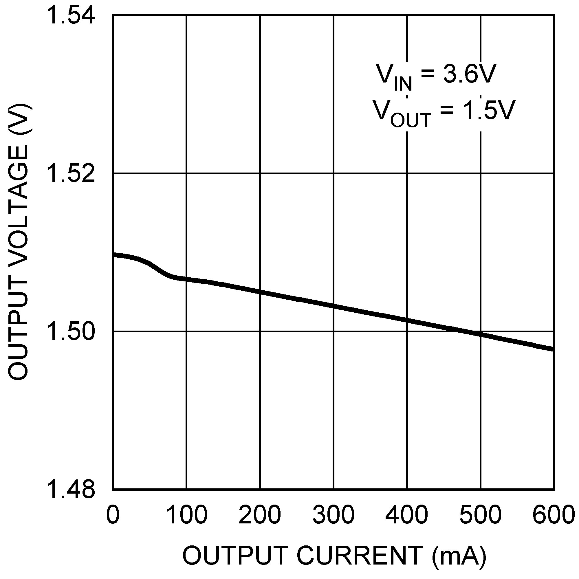 Figure 6. Output Voltage vs Output Current
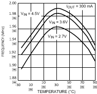 Figure 8. Switching Frequency vs Temperature
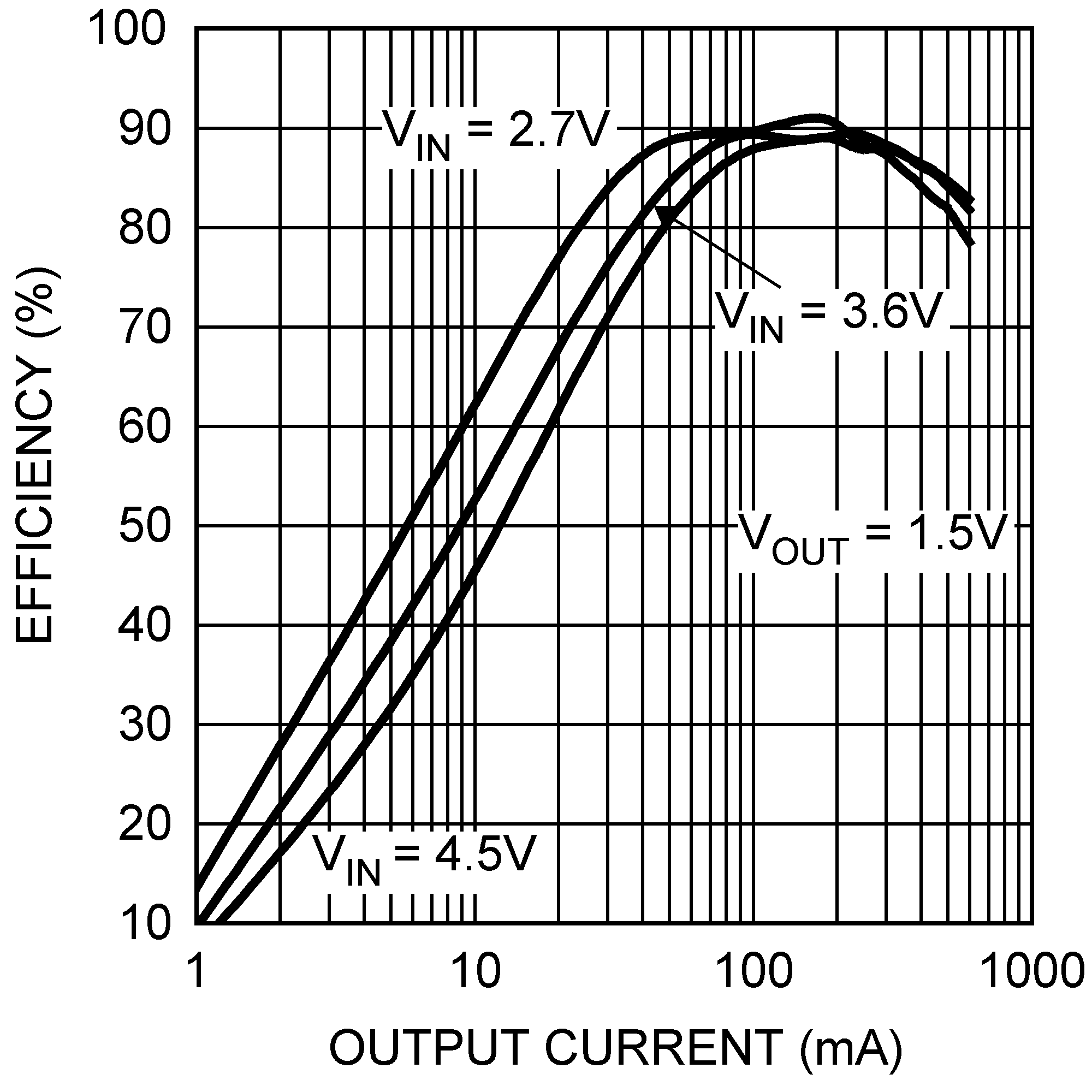
| VOUT = 1.5 V, L = 2.2 µH, DCR = 200 mΩ |
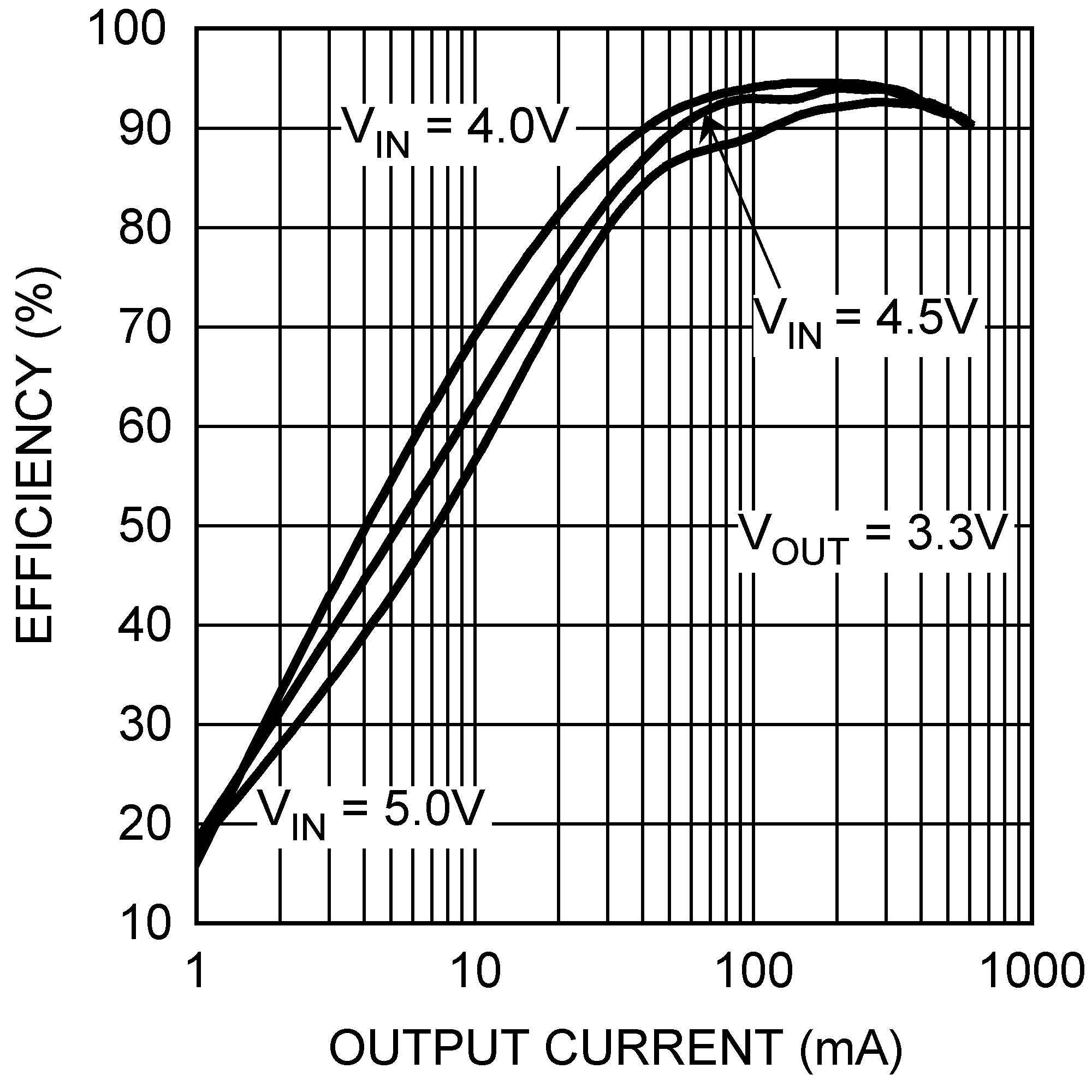
| VOUT = 3.3 V, L = 2.2 µH, DCR = 200 mΩ |
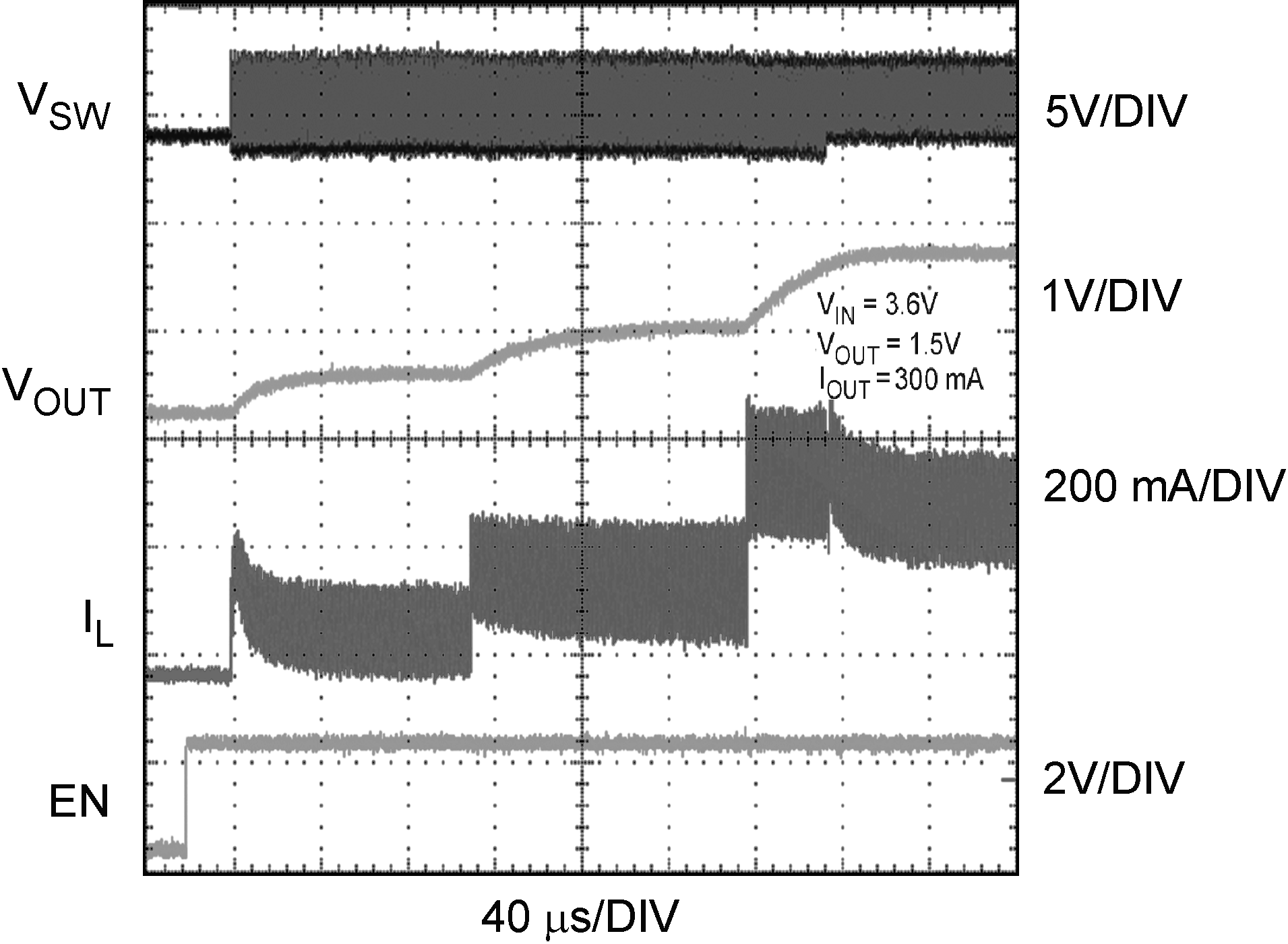
| Output Current = 300 mA |