SNVS506J May 2008 – December 2015 LM3691
PRODUCTION DATA.
- 1 Features
- 2 Applications
- 3 Description
- 4 Revision History
- 5 Voltage Options
- 6 Pin Configuration and Functions
- 7 Specifications
- 8 Detailed Description
- 9 Application and Implementation
- 10Power Supply Recommendations
- 11Layout
- 12Device and Documentation Support
- 13Mechanical, Packaging, and Orderable Information
8 Detailed Description
8.1 Overview
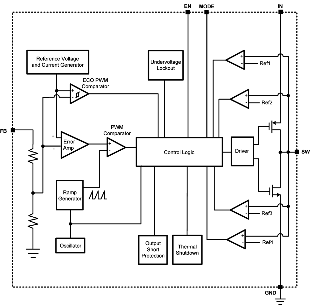
The LM3691, a high-efficiency, step-down DC-DC switching buck converter, delivers a constant voltage from either a single Li-Ion or three cell NiMH/NiCd battery to portable devices such as cell phones and PDAs. Using a voltage mode architecture with synchronous rectification, the LM3691 can deliver up to 1000 mA depending on the input voltage and output voltage, ambient temperature, and the inductor chosen.
There are three modes of operation depending on the current required: pulse width modulation (PWM), ECO, and shutdown. The device operates in PWM mode at load currents of approximately 50 mA (typical) or higher. Lighter output current loads cause the device to automatically switch into ECO mode for reduced current consumption and a longer battery life. Shutdown mode turns off the device, offering the lowest current consumption (ISHUTDOWN = 0.03 µA typical). Additional features include soft start, undervoltage protection, current overload protection, and thermal shutdown protection. As shown in Typical Application Circuit, only three external power components are required for implementation.
8.2 Functional Block Diagram

8.3 Feature Description
8.3.1 Circuit Operation
The LM3691 operates as follows. During the first portion of each switching cycle, the control block in the LM3691 turns on the internal PFET switch. This allows current to flow from the input through the inductor to the output filter capacitor and load. The inductor limits the current to a ramp with a slope of (VIN – VOUT)/L, by storing energy in a magnetic field. During the second portion of each cycle, the controller turns the PFET switch off, blocking current flow from the input, and then turns the NFET synchronous rectifier on. The inductor draws current from ground through the NFET to the output filter capacitor and load, which ramps the inductor current down with a slope of –VOUT/L.
The output filter stores charge when the inductor current is high, and releases it when low, smoothing the voltage across the load. The output voltage is regulated by modulating the PFET switch on time to control the average current sent to the load. The effect is identical to sending a duty-cycle modulated rectangular wave formed by the switch and synchronous rectifier at the SW pin to a low-pass filter formed by the inductor and output filter capacitor. The output voltage is equal to the average voltage at the SW pin.
8.3.2 PWM Operation
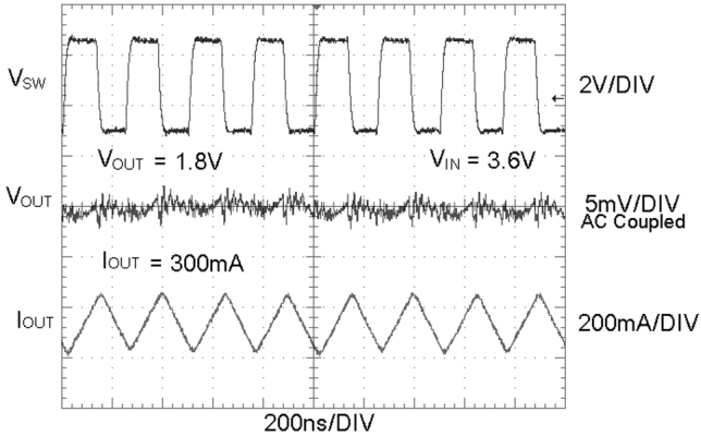
During PWM operation, the converter operates as a voltage-mode controller with input-voltage feed forward. This allows the converter to achieve excellent load and line regulation. The DC gain of the power stage is proportional to the input voltage. To eliminate this dependence, feed forward inversely proportional to the input voltage is introduced. While in PWM mode, the output voltage is regulated by switching at a constant frequency and then modulating the energy per cycle to control power to the load. At the beginning of each clock cycle the PFET switch is turned on, and the inductor current ramps up until the comparator trips and the control logic turns off the switch. The current limit comparator can also turn off the switch in case the current limit of the PFET is exceeded. Then the NFET switch is turned on, and the inductor current ramps down. The next cycle is initiated by the clock turning off the NFET and turning on the PFET.
 Figure 42. Typical PWM Operation
8.3.2.1 Internal Synchronous Rectification
While in PWM mode, the LM3691 uses an internal NFET as a synchronous rectifier to reduce rectifier forward voltage drop and associated power loss. Synchronous rectification provides a significant improvement in efficiency whenever the output voltage is relatively low compared to the voltage drop across an ordinary rectifier diode.
8.3.2.2 Current Limiting
A current limit feature allows the LM3691 to protect itself and external components during overload conditions. PWM mode implements current limit using an internal comparator that trips at 1500 mA (typical). If the output is shorted to ground, and the output voltage becomes lower than 0.3V (typical), the device enters a timed current-limit mode where the switching frequency is one fourth, and NFET synchronous rectifier is disabled, thus preventing excess current and thermal runaway.
8.3.3 ECO Operation
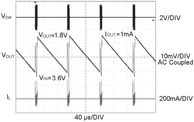
Setting the MODE pin low places the LM3691 in Auto mode. By doing so the part switches from ECOnomy (ECO) state to forced pulse width modulation (FPWM) state based on output load current. At light loads (less than 50 mA), the converter enters ECO mode. In this mode the part operates with low IQ. During ECO operation, the converter positions the output voltage slightly higher (30 mV typical) than the nominal output voltage in FPWM operation. Because the reference is set higher, the output voltage increases to reach the target voltage when the part goes from sleep state to switching state. Once this voltage is reached the converter enters sleep mode, thus reducing switching losses and improving light load efficiency. The output voltage ripple is slightly higher in ECO mode (30 mV peak-to-peak ripple typical).
 Figure 43. Typical ECO Operation
8.3.4 Soft-Start
The LM3691 has a soft-start circuit that limits in-rush current during start-up. Output voltage increase rate is
30 mV/µs (at VOUT = 1.8 V typical) during soft start.
8.3.5 Thermal Shutdown Protection
The LM3691 has a thermal overload protection function that operates to protect itself from short-term misuse and overload conditions. When the junction temperature exceeds around 150°C, the device inhibits operation. Both the PFET and the NFET are turned off. When the temperature drops below 130°C, normal operation resumes. Prolonged operation in thermal overload conditions may damage the device and is considered bad practice.
8.3.6 Overtemperature Maximum Load
Table 1. Maximum Overtemperature Load Recommendations
| VIN | MAXIMUM LOAD |
|---|---|
| 2.5 V to 5.5 V | 1000 mA |
| 2.3 V to 2.5 V | 650 mA |
8.4 Device Functional Modes
8.4.1 Forced PWM Mode
Setting the MODE pin high (> 1.2 V) places the LM3691 in FPWM. The device is in FPWM regardless of the load.
8.4.2 Shutdown Mode
Setting the EN input pin low (< 0.4 V) places the LM3691 in shutdown mode. During shutdown the PFET switch, NFET switch, reference, control and bias circuitry of the LM3691 are turned off. Setting EN high (> 1.2 V) enables normal operation. When turning on the device with EN soft start is activated. EN pin must be set low to turn off the LM3691 during system power up and undervoltage conditions when the supply is less than 2.3 V. Do not leave the EN pin floating.