SLCS162 June 2017 LM393-MIL
PRODUCTION DATA.
8 Application and Implementation
NOTE
Information in the following applications sections is not part of the TI component specification, and TI does not warrant its accuracy or completeness. TI’s customers are responsible for determining suitability of components for their purposes. Customers should validate and test their design implementation to confirm system functionality.
8.1 Application Information
LM393-MIL will typically be used to compare a single signal to a reference or two signals against each other. Many users take advantage of the open drain output to drive the comparison logic output to a logic voltage level to an MCU or logic device. The wide supply range and high voltage capability makes LM393-MIL optimal for level shifting to a higher or lower voltage.
8.2 Typical Application
 Figure 7. Single-Ended and Differential Comparator Configurations
8.2.1 Design Requirements
For this design example, use the parameters listed in Table 1 as the input parameters.
Table 1. Design Parameters
| DESIGN PARAMETER | EXAMPLE VALUE |
|---|---|
| Input Voltage Range | 0 V to Vsup-1.5 V |
| Supply Voltage | 2 V to 36 V |
| Logic Supply Voltage | 2 V to 36 V |
| Output Current (RPULLUP) | 1 μA to 20 mA |
| Input Overdrive Voltage | 100 mV |
| Reference Voltage | 2.5 V |
| Load Capacitance (CL) | 15 pF |
8.2.2 Detailed Design Procedure
When using LM393-MIL in a general comparator application, determine the following:
- Input Voltage Range
- Minimum Overdrive Voltage
- Output and Drive Current
- Response Time
8.2.2.1 Input Voltage Range
When choosing the input voltage range, the input common mode voltage range (VICR) must be taken in to account. If temperature operation is above or below 25°C the VICR can range from 0 V to VCC– 2.0 V. This limits the input voltage range to as high as VCC– 2.0 V and as low as 0 V. Operation outside of this range can yield incorrect comparisons.
Below is a list of input voltage situation and their outcomes:
- When both IN- and IN+ are both within the common-mode range:
- If IN- is higher than IN+ and the offset voltage, the output is low and the output transistor is sinking current
- If IN- is lower than IN+ and the offset voltage, the output is high impedance and the output transistor is not conducting
- When IN- is higher than common-mode and IN+ is within common-mode, the output is low and the output transistor is sinking current
- When IN+ is higher than common-mode and IN- is within common-mode, the output is high impedance and the output transistor is not conducting
- When IN- and IN+ are both higher than common-mode, the output is low and the output transistor is sinking current
8.2.2.2 Minimum Overdrive Voltage
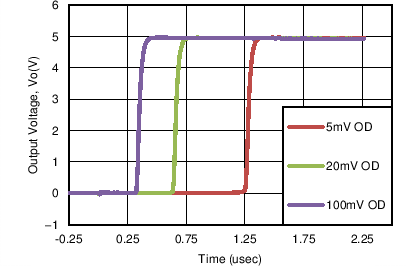
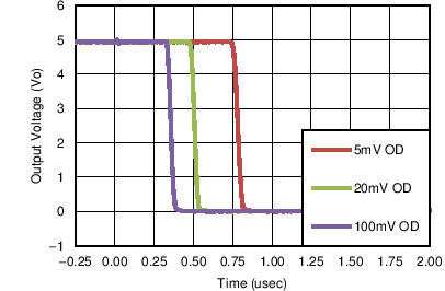
Overdrive Voltage is the differential voltage produced between the positive and negative inputs of the comparator over the offset voltage (VIO). To make an accurate comparison the Overdrive Voltage (VOD) should be higher than the input offset voltage (VIO). Overdrive voltage can also determine the response time of the comparator, with the response time decreasing with increasing overdrive. Figure 8 and Figure 9 show positive and negative response times with respect to overdrive voltage.
8.2.2.3 Output and Drive Current
Output current is determined by the load/pull-up resistance and logic/pullup voltage. The output current will produce a output low voltage (VOL) from the comparator. In which VOL is proportional to the output current. Use Typical Characteristics to determine VOL based on the output current.
The output current can also effect the transient response. See Response Time for more information.
8.2.2.4 Response Time
The transient response can be determined by the load capacitance (CL), load/pullup resistance (RPULLUP) and equivalent collector-emitter resistance (RCE)..
- The positive response time (τP) is approximately τP ~ RPULLUP × CL
- The negative response time (τN) is approximately τN ~ RCE × CL
- RCE can be determine by taking the slope of Typical Characteristics in its linear region at the desired temperature, or by dividing the VOL by Iout
8.2.3 Application Curves
The following curves were generated with 5 V on VCC and VLogic, RPULLUP = 5.1 kΩ, and 50 pF scope probe.
 Figure 8. Response Time for Various Overdrives
 (Positive Transition)
 Figure 9. Response Time for Various Overdrives
 (Negative Transition)