SLCS162 June   2017 LM393-MIL

PRODUCTION DATA.  

  1. Features
  2. Applications
  3. Description
  4. Revision History
  5. Pin Configuration and Functions
  6. Specifications
    1. 6.1 Absolute Maximum Ratings
    2. 6.2 ESD Ratings
    3. 6.3 Recommended Operating Conditions
    4. 6.4 Thermal Information
    5. 6.5 Electrical Characteristics
    6. 6.6 Switching Characteristics
    7. 6.7 Typical Characteristics
  7. Detailed Description
    1. 7.1 Overview
    2. 7.2 Functional Block Diagram
    3. 7.3 Feature Description
    4. 7.4 Device Functional Modes
      1. 7.4.1 Voltage Comparison
  8. Application and Implementation
    1. 8.1 Application Information
    2. 8.2 Typical Application
      1. 8.2.1 Design Requirements
      2. 8.2.2 Detailed Design Procedure
        1. 8.2.2.1 Input Voltage Range
        2. 8.2.2.2 Minimum Overdrive Voltage
        3. 8.2.2.3 Output and Drive Current
        4. 8.2.2.4 Response Time
      3. 8.2.3 Application Curves
  9. Power Supply Recommendations
  10. 10Layout
    1. 10.1 Layout Guidelines
    2. 10.2 Layout Example
  11. 11Device and Documentation Support
    1. 11.1 Receiving Notification of Documentation Updates
    2. 11.2 Community Resources
    3. 11.3 Trademarks
    4. 11.4 Electrostatic Discharge Caution
    5. 11.5 Glossary
  12. 12Mechanical, Packaging, and Orderable Information

封装选项

机械数据 (封装 | 引脚)
  • Y|0
散热焊盘机械数据 (封装 | 引脚)
订购信息

Layout

Layout Guidelines

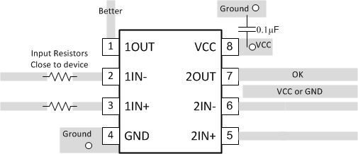
For accurate comparator applications without hysteresis it is important maintain a stable power supply with minimized noise and glitches, which can affect the high level input common-mode voltage range. To achieve this, it is best to add a bypass capacitor between the supply voltage and ground. This should be implemented on the positive power supply and negative supply (if available). If a negative supply is not being used, do not put a capacitor between the IC GND pin and system ground.

Layout Example

LM393-MIL lm393_layout.gif Figure 10. LM393-MIL Layout Example