SLCS162 June   2017 LM393-MIL

PRODUCTION DATA.  

  1. Features
  2. Applications
  3. Description
  4. Revision History
  5. Pin Configuration and Functions
  6. Specifications
    1. 6.1 Absolute Maximum Ratings
    2. 6.2 ESD Ratings
    3. 6.3 Recommended Operating Conditions
    4. 6.4 Thermal Information
    5. 6.5 Electrical Characteristics
    6. 6.6 Switching Characteristics
    7. 6.7 Typical Characteristics
  7. Detailed Description
    1. 7.1 Overview
    2. 7.2 Functional Block Diagram
    3. 7.3 Feature Description
    4. 7.4 Device Functional Modes
      1. 7.4.1 Voltage Comparison
  8. Application and Implementation
    1. 8.1 Application Information
    2. 8.2 Typical Application
      1. 8.2.1 Design Requirements
      2. 8.2.2 Detailed Design Procedure
        1. 8.2.2.1 Input Voltage Range
        2. 8.2.2.2 Minimum Overdrive Voltage
        3. 8.2.2.3 Output and Drive Current
        4. 8.2.2.4 Response Time
      3. 8.2.3 Application Curves
  9. Power Supply Recommendations
  10. 10Layout
    1. 10.1 Layout Guidelines
    2. 10.2 Layout Example
  11. 11Device and Documentation Support
    1. 11.1 Receiving Notification of Documentation Updates
    2. 11.2 Community Resources
    3. 11.3 Trademarks
    4. 11.4 Electrostatic Discharge Caution
    5. 11.5 Glossary
  12. 12Mechanical, Packaging, and Orderable Information

封装选项

机械数据 (封装 | 引脚)
  • Y|0
散热焊盘机械数据 (封装 | 引脚)
订购信息

Pin Configuration and Functions

D, DGK, P, PS, or PW
8-Pin SOIC, VSSOP, PDIP, SO, or TSSOP
Top View
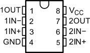
LM393-MIL po_lcs005.gif

Pin Functions

PIN I/O DESCRIPTION
NAME SOIC, VSSOP, PDIP, SO, and TSSOP
1OUT 1 Output Output pin of comparator 1
1IN– 2 Input Negative input pin of comparator 1
1IN+ 3 Input Positive input pin of comparator 1
GND 4 Ground
2IN+ 5 Input Positive input pin of comparator 2
2IN- 6 Input Negative input pin of comparator 2
2OUT 7 Output Output pin of comparator 2
VCC 8 Supply Pin