SNOS977F May 2001 – May 2016 LM397
PRODUCTION DATA.
7 Detailed Description
7.1 Overview
A comparator is often used to convert an analog signal to a digital signal. The comparator compares an input voltage (VIN) at the noninverting pin to the reference voltage (VREF) at the inverting pin. If VIN is less than VREF the output (VO) is low (VOL). However, if VIN is greater than VREF, the output voltage (VO) is high (VOH). Refer to Figure 6.
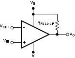 Figure 5. Basic Comparator
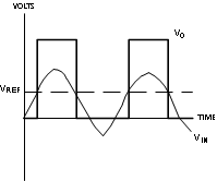 Figure 6. Basic Comparator Output
7.2 Functional Block Diagram
7.3 Feature Description
7.3.1 Input Stage
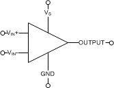
The LM397 has a bipolar input stage. The input common-mode voltage range is from 0 to (VS – 1.5 V).
7.3.2 Output Stage
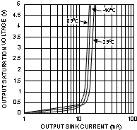
The LM397 has an open-collector grounded-emitter NPN output transistor for the output stage. This requires an external pullup resistor connected between the positive supply voltage and the output. The external pullup resistor should be high enough resistance so to avoid excessive power dissipation. In addition, the pullup resistor should be low enough resistance to enable the comparator to switch with the load circuitry connected. Because it is an open-collector output stage, several comparator outputs can be connected together to create an OR’ing function output. With an open collector, the output can be used as a simple SPST switch to ground. The amount of current which the output can sink is approximately 10 mA. When the maximum current limit is reached, the output transistor will saturate and the output will rise rapidly (Figure 7).
7.4 Device Functional Modes
7.4.1 Hysteresis
The basic comparator configuration may oscillate or produce a noisy output if the applied differential input is near the input offset voltage of the comparator. This tends to occur when the voltage on the input is equal or very close to the other input voltage. Adding hysteresis can prevent this problem. Hysteresis creates two switching thresholds (one for the rising input voltage and the other for the falling input voltage). Hysteresis is the voltage difference between the two switching thresholds. When both inputs are nearly equal, hysteresis causes one input to effectively move quickly pass the other. Thus, effectively moving the input out of region that oscillation may occur.
For an inverting configured comparator, hysteresis can be added with a three resistor network and positive feedback. When input voltage (VIN) at the inverting node is less than non-inverting node (VT), the output is high. The equivalent circuit for the three resistor network is R1 in parallel with R3 and in series with R2. The lower threshold voltage VT1 is calculated by Equation 1:
When VIN is greater than VT, the output voltage is low. The equivalent circuit for the three resistor network is R2 in parallel with R3 and in series with R1. The upper threshold voltage VT2 is calculated by Equation 2:
The hysteresis is defined in Equation 3:
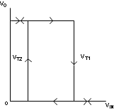 Figure 8. Inverting Configured Comparator - LM397
