SNOS455G May 2000 – September 2015 LM4050-N , LM4050-N-Q1
PRODUCTION DATA.
- 1 Features
- 2 Applications
- 3 Description
- 4 Revision History
- 5 Pin Configuration and Functions
-
6 Specifications
- 6.1 Absolute Maximum Ratings
- 6.2 ESD Ratings
- 6.3 Recommended Operating Conditions
- 6.4 Thermal Information
- 6.5 Electrical Characteristics: 2-V Option
- 6.6 Electrical Characteristics: 2.5-V Option
- 6.7 Electrical Characteristics: 4.1-V Option
- 6.8 Electrical Characteristics: 5-V Option
- 6.9 Electrical Characteristics: 8.2-V Option
- 6.10 Electrical Characteristics: 10-V Option
- 6.11 Typical Characteristics
- 7 Parameter Measurement Information
- 8 Detailed Description
- 9 Application and Implementation
- 10Power Supply Recommendations
- 11Layout
- 12Device and Documentation Support
- 13Mechanical, Packaging, and Orderable Information
6 Specifications
6.1 Absolute Maximum Ratings
See (1),(2)| MIN | MAX | UNIT | |||
|---|---|---|---|---|---|
| Reverse Current | 20 | mA | |||
| Forward Current | 10 | mA | |||
| Power Dissipation (TA = 25°C)(1) | 280 | mW | |||
| Maximum Junction Temperature (2) | 150 | °C | |||
| Storage Temperature | –65 | 150 | °C | ||
(1) Stresses beyond those listed under Absolute Maximum Ratings may cause permanent damage to the device. These are stress ratings only, which do not imply functional operation of the device at these or any other conditions beyond those indicated under Recommended Operating Conditions. Exposure to absolute-maximum-rated conditions for extended periods may affect device reliability.
(2) If Military/Aerospace specified devices are required, please contact the Texas Instruments Sales Office/ Distributors for availability and specifications.
6.2 ESD Ratings
| VALUE | UNIT | |||
|---|---|---|---|---|
| V(ESD) | Electrostatic discharge | Human body model (HBM), per ANSI/ESDA/JEDEC JS-001(1) | ±2000 | V |
| Charged device model (CDM), per JEDEC specification JESD22-C101(2) | ±1000 | |||
| Machine model (MM) | ±200 | |||
(1) JEDEC document JEP155 states that 500-V HBM allows safe manufacturing with a standard ESD control process.
(2) JEDEC document JEP157 states that 250-V CDM allows safe manufacturing with a standard ESD control process.
6.3 Recommended Operating Conditions
over operating free-air temperature range (unless otherwise noted) (1)(1)| MIN | MAX | UNIT | ||
|---|---|---|---|---|
| Industrial Temperature Range | Ambient Temperature Range | –40 | 85 | °C |
| Junction Temperature Range | –40 | 85 | °C | |
| Extended Temperature Range | Ambient Temperature Range | –40 | 125 | °C |
| Junction Temperature | –40 | 125 | °C | |
6.4 Thermal Information
| THERMAL METRIC(1) | LM4050-N/-Q1 | UNIT | |
|---|---|---|---|
| DBZ (SOT-23) | |||
| 3 PINS | |||
| RθJA | Junction-to-ambient thermal resistance | 287 | °C/W |
| RθJC(top) | Junction-to-case (top) thermal resistance | 106.6 | °C/W |
| RθJB | Junction-to-board thermal resistance | 57.7 | °C/W |
| ψJT | Junction-to-top characterization parameter | 5.5 | °C/W |
| ψJB | Junction-to-board characterization parameter | 56.4 | °C/W |
| RθJC(bot) | Junction-to-case (bottom) thermal resistance | N/A | °C/W |
(1) For more information about traditional and new thermal metrics, see the Semiconductor and IC Package Thermal Metrics application report, SPRA953.
6.5 Electrical Characteristics: 2-V Option
All other limits TA = TJ = 25°C. The grades A, B and C designate initial Reverse Breakdown Voltage tolerances of ±0.1%, ±0.2%, and 0.5% respectively.| PARAMETER | TEST CONDITIONS | MIN(4) | TYP(3) | MAX(4) | UNIT | ||
|---|---|---|---|---|---|---|---|
| VR | Reverse Breakdown Voltage | IR = 100 μA | 2.048 | V | |||
| Reverse breakdown voltage tolerance(5) | IR = 100 μA | LM4050AIM3, LM4050AEM3 | ±2.048 | mV | |||
| LM4050BIM3, LM4050BEM3 | ±4.096 | ||||||
| LM4050CIM3, LM4050CEM3 | ±1024 | ||||||
| Industrial temperature range TA = TJ = TMIN to TMAX |
LM4050AIM3, LM4050AEM3 | ±9.0112 | |||||
| LM4050BIM3, LM4050BEM3 | ±11.4688 | ||||||
| LM4050CIM3, LM4050CEM3 | ±14.7456 | ||||||
| Extended temperature range TA = TJ = TMIN to TMAX |
LM4050AIM3, LM4050AEM3 | ±12.288 | |||||
| LM4050BIM3, LM4050BEM3 | ±14.7456 | ||||||
| LM4050CIM3, LM4050CEM3 | ±17.2032 | ||||||
| IRMIN | Minimum operating current | TA = TJ = 25°C | 41 | 60 | μA | ||
| TA = TJ = TMIN to TMAX | 65 | ||||||
| ΔVR/ΔT | Average reverse breakdown voltage temperature coefficient(5) | IR = 10 mA | ±20 | ppm/°C | |||
| IR = 1 mA | ±15 | ||||||
| IR = 100 μA, TA = TJ = 25°C | ±15 | ||||||
| IR = 100 μA, TA = TJ = TMIN to TMAX |
±50 | ||||||
| ΔVR/ΔIR | Reverse breakdown voltage change with operating current change(6) | IRMIN ≤ IR ≤ 1 mA, TA = TJ = 25°C | 0.3 | 0.8 | mV | ||
| IRMIN ≤ IR ≤ 1 mA, TA = TJ = TMIN to TMAX |
1.2 | ||||||
| 1 mA ≤ IR ≤ 15 mA, TA = TJ = 25°C | 2.3 | 6 | |||||
| 1 mA ≤ IR ≤ 15 mA, TA = TJ = TMIN to TMAX |
8 | ||||||
| ZR | Reverse dynamic impedance | IR = 1 mA, f = 120 Hz, IAC = 0.1 IR | 0.3 | Ω | |||
| eN | Wideband noise | IR = 100 μA, 10 Hz ≤ f ≤ 10 kHz | 34 | μVrms | |||
| ΔVR | Reverse breakdown voltage long term stability | t = 1000 hrs, T = 25°C ±0.1°C, IR = 100 μA | 120 | ppm | |||
| VHYST | Thermal hysteresis (7) | ΔT = −40°C to 125°C | 0.7 | mV | |||
6.6 Electrical Characteristics: 2.5-V Option
All other limits TA = TJ = 25°C. The grades A, B and C designate initial Reverse Breakdown Voltage tolerances of ±0.1%, ±0.2%, and 0.5% respectively.| PARAMETER | TEST CONDITIONS | MIN(4) | TYP(3) | MAX(4) | UNIT | ||
|---|---|---|---|---|---|---|---|
| VR | Reverse breakdown voltage | IR = 100 μA | 2.500 | V | |||
| IR = 100 μA | LM4050AIM3, LM4050AEM3 | ±2.5 | mV | ||||
| LM4050BIM3, LM4050BEM3 | ±5 | ||||||
| LM4050CIM3, LM4050CEM3 | ±13 | ||||||
| Reverse breakdown voltage tolerance(5) | Industrial temperature range, TA = TJ = TMIN to TMAX |
LM4050AIM3, LM4050AEM3 | ±11 | mV | |||
| LM4050BIM3, LM4050BEM3 | ±24 | ||||||
| LM4050CIM3, LM4050CEM3 | ±21 | ||||||
| Extended temperature range, TA = TJ = TMIN to TMAX |
LM4050AIM3, LM4050AEM3 | ±15 | |||||
| LM4050BIM3, LM4050BEM3 | ±18 | ||||||
| LM4050CIM3, LM4050CEM3 | ±25 | ||||||
| IRMIN | Minimum operating current | TA = TJ = 25°C | 41 | 60 | μA | ||
| TA = TJ = TMIN to TMAX | 65 | ||||||
| ΔVR/ΔT | Average reverse breakdown voltage temperature coefficient(5) | IR = 10 mA | ±20 | ppm/°C | |||
| IR = 1 mA | ±15 | ||||||
| IR = 100 μA, TA = TJ = 25°C | ±15 | ||||||
| IR = 100 μA, TA = TJ = TMIN to TMAX |
±50 | ||||||
| ΔVR/ΔIR | Reverse breakdown voltage change with operating current change(6) | IRMIN ≤ IR ≤ 1 mA, TA = TJ = 25°C | 0.3 | 0.8 | mV | ||
| IRMIN ≤ IR ≤ 1 mA TA = TJ = TMIN to TMAX |
1.2 | ||||||
| ΔVR/ΔIR | Reverse breakdown voltage change with operating current change(6) | 1 mA ≤ IR ≤ 15 mA, TA = TJ = 25°C | 2.3 | 6 | mV | ||
| 1 mA ≤ IR ≤ 15 mA, TA = TJ = TMIN to TMAX |
8 | ||||||
| ZR | Reverse dynamic impedance | IR = 1 mA, f = 120 Hz, IAC = 0.1 IR | 0.3 | Ω | |||
| eN | Wideband noise | IR = 100 μA, 10 Hz ≤ f ≤ 10 kHz | 41 | μVrms | |||
| ΔVR | Reverse breakdown voltage long term stability | t = 1000 hrs, T = 25°C ±0.1°C, IR = 100 μA | 120 | ppm | |||
| VHYST | Thermal hysteresis (7) | ΔT = −40°C to 125°C | 07 | mV | |||
6.7 Electrical Characteristics: 4.1-V Option
All other limits TA = TJ = 25°C. The grades A, B and C designate initial Reverse Breakdown Voltage tolerances of ±0.1%, ±0.2%, and 0.5% respectively.| PARAMETER | TEST CONDITIONS | MIN | TYP(3) | MAX | UNIT | ||
|---|---|---|---|---|---|---|---|
| VR | Reverse Breakdown Voltage | IR = 100 μA | 4.096 | V | |||
| Reverse Breakdown Voltage Tolerance(5) | IR = 100 μA | LM4050AIM3, LM4050AEM3 | ±4.1 | mV | |||
| LM4050BIM3,LM4050BEM3 | ±8.2 | ||||||
| LM4050CIM3, LM4050CEM3 | ±21 | ||||||
| Industrial temperature range, TA = TJ = TMIN to TMAX |
LM4050AIM3, LM4050AEM3 | ±18 | |||||
| LM4050BIM3,LM4050BEM3 | ±22 | ||||||
| LM4050CIM3, LM4050CEM3 | ±34 | ||||||
| Extended temperature range, TA = TJ = TMIN to TMAX |
LM4050AIM3, LM4050AEM3 | ±25 | |||||
| LM4050BIM3,LM4050BEM3 | ±29 | ||||||
| LM4050CIM3, LM4050CEM3 | ±41 | ||||||
| IRMIN | Minimum Operating Current | TA = TJ = 25°C | 52 | 68 | μA | ||
| Industrial temperature range, TA = TJ = TMIN to TMAX |
73 | ||||||
| Extended temperature range, TA = TJ = TMIN to TMAX |
78 | ||||||
| ΔVR/ΔT | Average reverse breakdown voltage temperature coefficient(5) | IR = 10 mA | ±30 | ppm/°C | |||
| IR = 1 mA | ±20 | ||||||
| IR = 100 μA, TA = TJ = 25°C | ±20 | ||||||
| IR = 100 μA, TA = TJ = TMIN to TMAX |
±50 | ||||||
| ΔVR/ΔIR | Reverse breakdown voltage change with operating current change(6) | IRMIN ≤ IR ≤ 1 mA, TA = TJ = 25°C | 0.2 | 0.9 | mV | ||
| IRMIN ≤ IR ≤ 1 mA, TA = TJ = TMIN to TMAX |
1.2 | ||||||
| 1 mA ≤ IR ≤ 15 mA, TA = TJ = 25°C | 2 | 7 | |||||
| 1 mA ≤ IR ≤ 15 mA, TA = TJ = TMIN to TMAX |
10 | ||||||
| ZR | Reverse dynamic impedance | IR = 1 mA, f = 120 Hz, IAC = 0.1 IR | 0.5 | Ω | |||
| eN | Wideband noise | IR = 100 μA, 10 Hz ≤ f ≤ 10 kHz | 93 | μVrms | |||
| ΔVR | Reverse breakdown voltage long term stability | t = 1000 hrs, T = 25°C ±0.1°C, IR = 100 μA | 120 | ppm | |||
| VHYST | Thermal hysteresis(7) | ΔT = −40°C to 125°C | 1.148 | mV | |||
6.8 Electrical Characteristics: 5-V Option
All other limits TA = TJ = 25°C. The grades A, B and C designate initial Reverse Breakdown Voltage tolerances of ±0.1%, ±0.2% and 0.5% respectively.| PARAMETER | TEST CONDITIONS | MIN(4) | TYP(3) | MAX(4) | UNIT | ||
|---|---|---|---|---|---|---|---|
| VR | Reverse Breakdown Voltage | IR = 100 μA | 5 | V | |||
| Reverse Breakdown Voltage Tolerance(5) | IR = 100 μA | LM4050AIM3, LM4050AEM3 | ±5 | mV | |||
| LM4050BIM3. LM4050BEM3 | ±10 | ||||||
| LM4050CIM3, LM4050CEM3 | ±25 | ||||||
| Industrial Temp. Range TA = TJ = TMIN to TMAX |
LM4050AIM3, LM4050AEM3 | ±22 | |||||
| LM4050BIM3, LM4050BEM3 | ±27 | ||||||
| LM4050CIM3, LM4050CEM3 | ±42 | ||||||
| Extended Temp. Range TA = TJ = TMIN to TMAX |
LM4050AIM3, LM4050AEM3 | ±30 | |||||
| LM4050BIM3, LM4050BEM3 | ±35 | ||||||
| LM4050CIM3, LM4050CEM3 | ±50 | ||||||
| IRMIN | Minimum Operating Current | TA = TJ = 25°C | 56 | 74 | μA | ||
| Industrial Temp. Range TA = TJ = TMIN to TMAX |
80 | ||||||
| Extended Temp. Range TA = TJ = TMIN to TMAX |
90 | ||||||
| ΔVR/ΔT | Average Reverse Breakdown Voltage Temperature Coefficient(5) | IR = 10 mA | ±30 | ppm/°C | |||
| IR = 1 mA | ±20 | ||||||
| IR = 100 μA, TA = TJ = 25°C | ±20 | ||||||
| IR = 100 μA TA = TJ = TMIN to TMAX |
±50 | ||||||
| ΔVR/ΔIR | Reverse Breakdown Voltage Change with Operating Current Change(6) | IRMIN ≤ IR ≤ 1 mA, TA = TJ = 25°C | 0.2 | 1 | mV | ||
| IRMIN ≤ IR ≤ 1 mA TA = TJ = TMIN to TMAX |
1.4 | ||||||
| 1 mA ≤ IR ≤ 15 mA, TA = TJ = 25°C | 2 | 8 | |||||
| 1 mA ≤ IR ≤ 15 mA TA = TJ = TMIN to TMAX |
12 | ||||||
| ZR | Reverse Dynamic Impedance | IR = 1 mA, f = 120 Hz | 0.5 | Ω | |||
| IAC = 0.1 IR | |||||||
| eN | Wideband Noise | IR = 100 μA 10 Hz ≤ f ≤ 10 kHz |
93 | μVrms | |||
| ΔVR | Reverse Breakdown Voltage Long Term Stability | t = 1000 hrs T = 25°C ±0.1°C IR = 100 μA |
120 | ppm | |||
| VHYST | Thermal Hysteresis(7) | ΔT = –40°C to 125°C | 1.4 | mV | |||
6.9 Electrical Characteristics: 8.2-V Option
All other limits TA = TJ = 25°C. The grades A, B and C designate initial Reverse Breakdown Voltage tolerances of ±0.1% and ±0.2% and 0.5% respectively.| PARAMETER | TEST CONDITIONS | MIN(4) | TYP(3) | MAX(4) | UNIT | ||
|---|---|---|---|---|---|---|---|
| VR | Reverse Breakdown Voltage | IR = 150 μA | 8.192 | V | |||
| Reverse Breakdown Voltage Tolerance (5) | IR = 150 μA | LM4050AIM3, LM4050AEM3 | ±8.2 | mV | |||
| LM4050BIM3, LM4050BEM3 | ±16 | ||||||
| LM4050CIM3, LM4050CEM3 | ±41 | ||||||
| Industrial Temp. Range TA = TJ = TMIN to TMAX |
LM4050AIM3, LM4050AEM3 | ±35 | |||||
| LM4050BIM3, LM4050BEM3 | ±43 | ||||||
| LM4050CIM3, LM4050CEM3 | ±68 | ||||||
| Extended Temp. Range TA = TJ = TMIN to TMAX |
LM4050AIM3, LM4050AEM3 | ±49 | |||||
| LM4050BIM3, LM4050BEM3 | ±57 | ||||||
| LM4050CIM3, LM4050CEM3 | ±82 | ||||||
| IRMIN | Minimum Operating Current | TA = TJ = 25°C | 74 | 91 | μA | ||
| Industrial Temp. Range TA = TJ = TMIN to TMAX |
95 | ||||||
| Extended Temp. Range TA = TJ = TMIN to TMAX |
100 | ||||||
| ΔVR/ΔT | Average Reverse Breakdown Voltage Temperature Coefficient (5) | IR = 10 mA | ±40 | ppm/°C | |||
| IR = 1 mA | ±20 | ||||||
| IR = 150 μA, TA = TJ = 25°C | ±20 | ||||||
| IR = 150 μA TA = TJ = TMIN to TMAX |
±50 | ||||||
| ΔVR/ΔIR | Reverse Breakdown Voltage Change with Operating Current Change (6) | IRMIN ≤ IR ≤ 1 mA, TA = TJ = 25°C | 0.6 | 1.3 | mV | ||
| IRMIN ≤ IR ≤ 1 mA TA = TJ = TMIN to TMAX |
2.5 | ||||||
| 1 mA ≤ IR ≤ 15 mA, TA = TJ = 25°C | 7 | 10 | |||||
| 1 mA ≤ IR ≤ 15 mA TA = TJ = TMIN to TMAX |
18 | ||||||
| ZR | Reverse Dynamic Impedance | IR = 1 mA, f = 120 Hz, IAC = 0.1 IR |
0.6 | Ω | |||
| eN | Wideband Noise | IR = 150 μA 10 Hz ≤ f ≤ 10 kHz |
150 | μVrms | |||
| ΔVR | Reverse Breakdown Voltage Long Term Stability | t = 1000 hrs T = 25°C ±0.1°C IR = 150 μA |
120 | ppm | |||
| VHYST | Thermal Hysteresis (7) |
ΔT = −40°C to 125°C | 2.3 | mV | |||
6.10 Electrical Characteristics: 10-V Option
All other limits TA = TJ = 25°C. The grades A, B and C designate initial Reverse Breakdown Voltage tolerances of ±0.1% and ±0.2% and 0.5% respectively.| PARAMETER | TEST CONDITIONS | MIN(4) | TYP(3) | MAX(4) | UNIT | ||
|---|---|---|---|---|---|---|---|
| VR | Reverse Breakdown Voltage | IR = 150 μA | 10 | V | |||
| Reverse Breakdown Voltage Tolerance (5) | IR = 150 μA | LM4050AIM3, LM4050AEM3 | ±10 | mV (max) | |||
| LM4050BIM3, LM4050BEM3 | ±20 | ||||||
| LM4050CIM3, LM4050CEM3 | ±50 | ||||||
| Industrial Temp. Range TA = TJ = TMIN to TMAX |
LM4050AIM3, LM4050AEM3 | ±43 | |||||
| LM4050BIM3, LM4050BEM3 | ±53 | ||||||
| LM4050CIM3, LM4050CEM3 | ±83 | ||||||
| Extended Temp. Range TA = TJ = TMIN to TMAX |
LM4050AIM3, LM4050AEM3 | ±60 | |||||
| LM4050BIM3, LM4050BEM3 | ±70 | ||||||
| LM4050CIM3, LM4050CEM3 | ±100 | ||||||
| IRMIN | Minimum Operating Current | TA = TJ = 25°C | 80 | 100 | μA | ||
| Industrial Temp. Range TA = TJ = TMIN to TMAX |
103 | ||||||
| Extended Temp. Range TA = TJ = TMIN to TMAX |
110 | ||||||
| ΔVR/ΔT | Average Reverse Breakdown Voltage Temperature Coefficient (5) | IR = 10 mA | ±40 | ppm/°C | |||
| IR = 1 mA | ±20 | ||||||
| IR = 150 μA, TA = TJ = 25°C | ±20 | ||||||
| IR = 150 μA TA = TJ = TMIN to TMAX |
±50 | ||||||
| ΔVR/ΔIR | Reverse Breakdown Voltage Change with Operating Current Change (6) | IRMIN ≤ IR ≤ 1 mA, TA = TJ = 25°C | 0.8 | 1.5 | mV | ||
| IRMIN ≤ IR ≤ 1 mA TA = TJ = TMIN to TMAX |
3.5 | ||||||
| 1 mA ≤ IR ≤ 15 mA, TA = TJ = 25°C | 8 | 12 | |||||
| 1 mA ≤ IR ≤ 15 mA TA = TJ = TMIN to TMAX |
23 | ||||||
| ZR | Reverse Dynamic Impedance | IR = 1 mA, f = 120 Hz, IAC = 0.1 IR |
0.7 | Ω | |||
| eN | Wideband Noise | IR = 150 μA 10 Hz ≤ f ≤ 10 kHz |
150 | μVrms | |||
| ΔVR | Reverse Breakdown Voltage Long Term Stability | t = 1000 hrs T = 25°C ±0.1°C IR = 150 μA |
120 | ppm | |||
| VHYST | Thermal Hysteresis(7) | ΔT = −40°C to 125°C | 2.8 | mV | |||
(1) The maximum power dissipation must be derated at elevated temperatures and is dictated by TJmax (maximum junction temperature), RθJA (junction to ambient thermal resistance), and TA (ambient temperature). The maximum allowable power dissipation at any temperature is PDmax = (TJmax − TA)/RθJA or the number given in the Absolute Maximum Ratings, whichever is lower. For the LM4050-N, TJmax = 150°C, and the typical thermal resistance (RθJA), when board mounted, is 326°C/W for the SOT-23 package.
(2) High junction temperatures degrade operating lifetimes. Operating lifetime is de-rated for junction temperatures greater than 125°C.
(3) Typicals are at TJ = 25°C and represent most likely parametric norm.
(4) Limits are 100% production tested at 25°C. Limits over temperature are guaranteed through correlation using Statistical Quality Control (SQC) methods. The limits are used to calculate National's AOQL.
(5) The overtemperature limit for Reverse Breakdown Voltage Tolerance is defined as the room temperature Reverse Breakdown Voltage Tolerance ±[(ΔV R/ΔT)(maxΔT)(VR)]. Where, ΔVR/ΔT is the VR temperature coefficient, maxΔT is the maximum difference in temperature from the reference point of 25°C to T MIN or TMAX, and VR is the reverse breakdown voltage. The total overtemperature tolerance for the different grades in the industrial temperature range where maxΔT = 65°C is shown below: A-grade: ±0.425% = ±0.1% ±50 ppm/°C × 65°C B-grade: ±0.525% = ±0.2% ±50 ppm/°C × 65°C C-grade: ±0.825% = ±0.5% ±50 ppm/°C × 65°C. Therefore, as an example, the A-grade LM4050-N-2.5 has an overtemperature Reverse Breakdown Voltage tolerance of ±2.5V × 0.425% = ±11 mV.
(6) Load regulation is measured on pulse basis from no load to the specified load current. Output changes due to die temperature change must be taken into account separately.
(7) Thermal hysteresis is defined as the difference in voltage measured at 25°C after cycling to temperature –40°C and the 25°C measurement after cycling to temperature 125°C.
6.11 Typical Characteristics
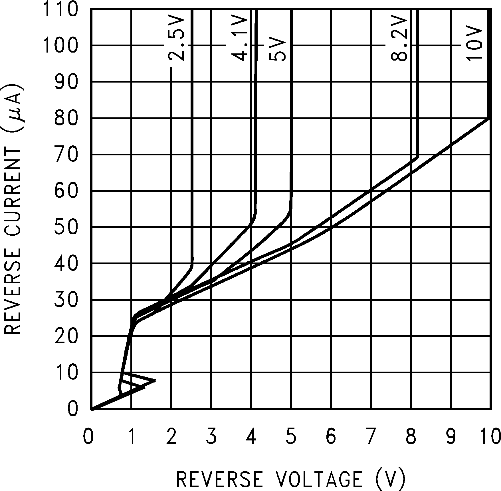
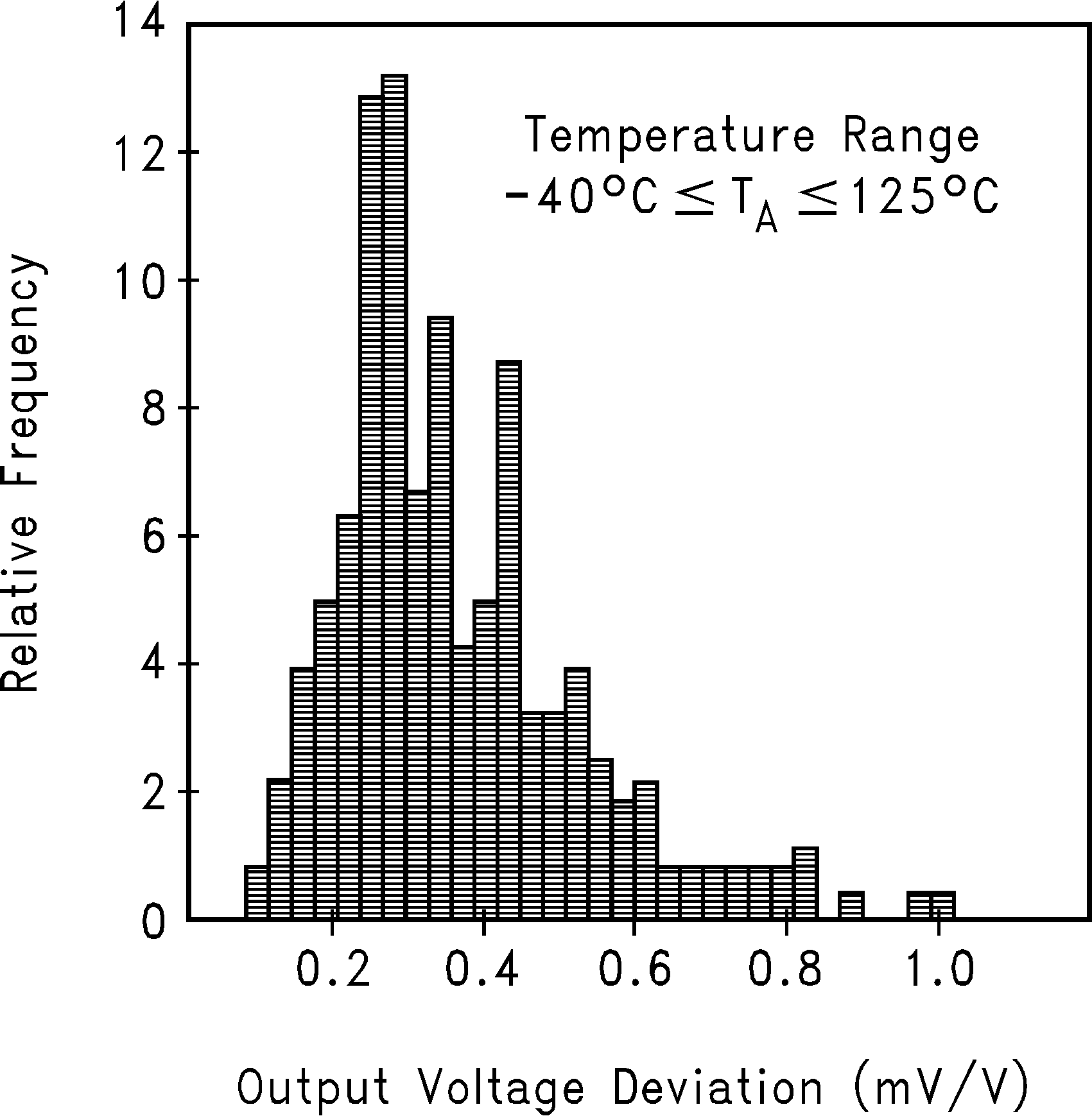
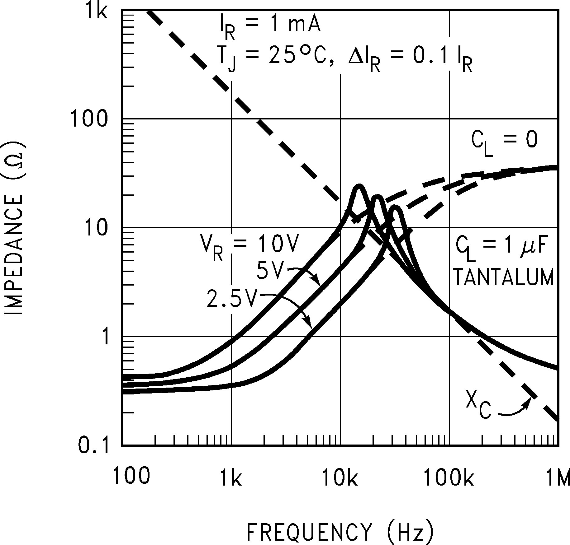
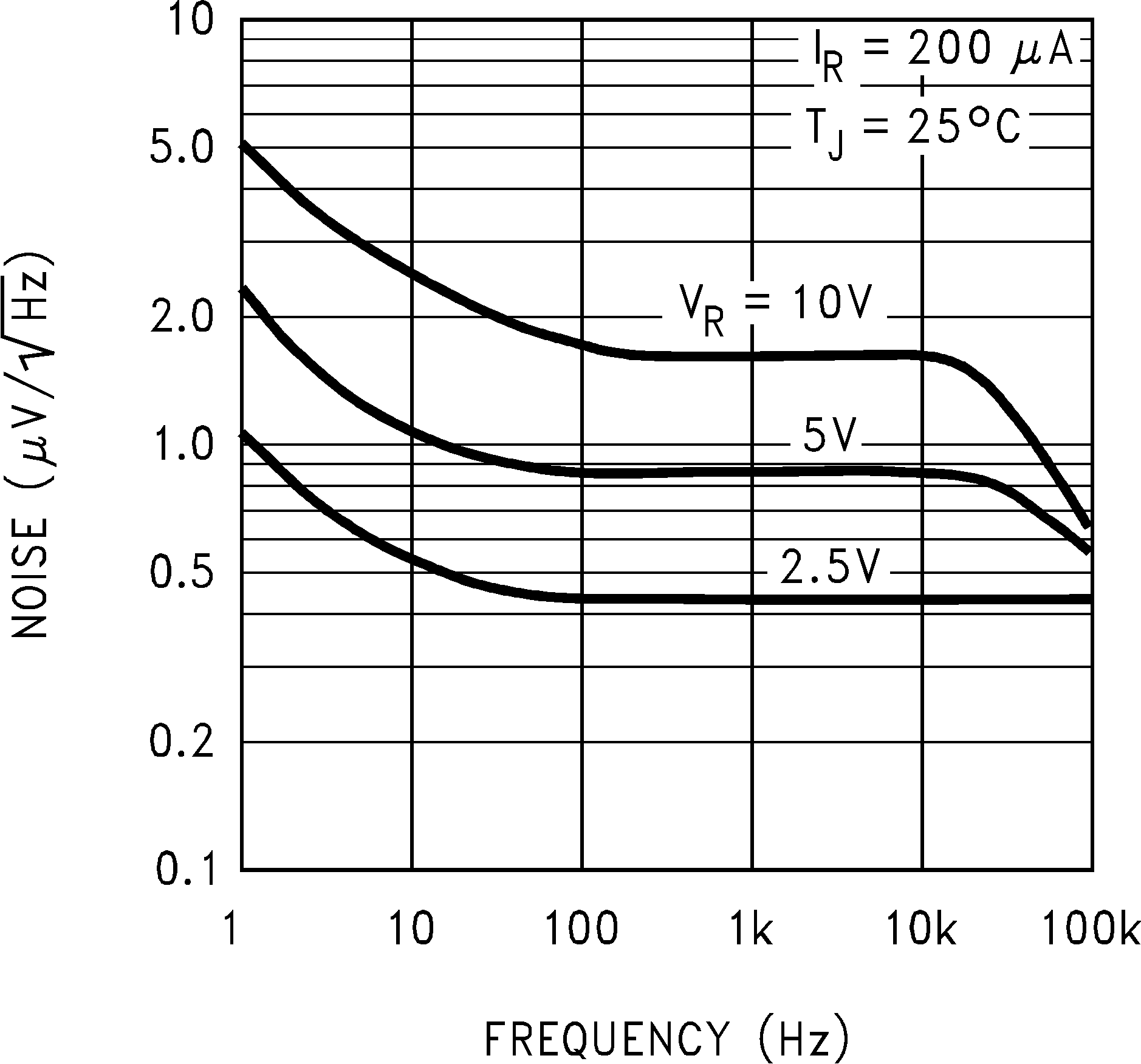
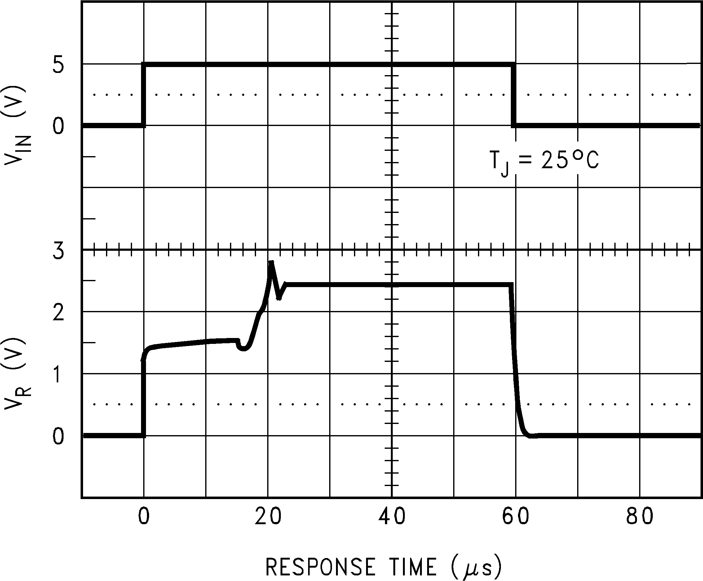
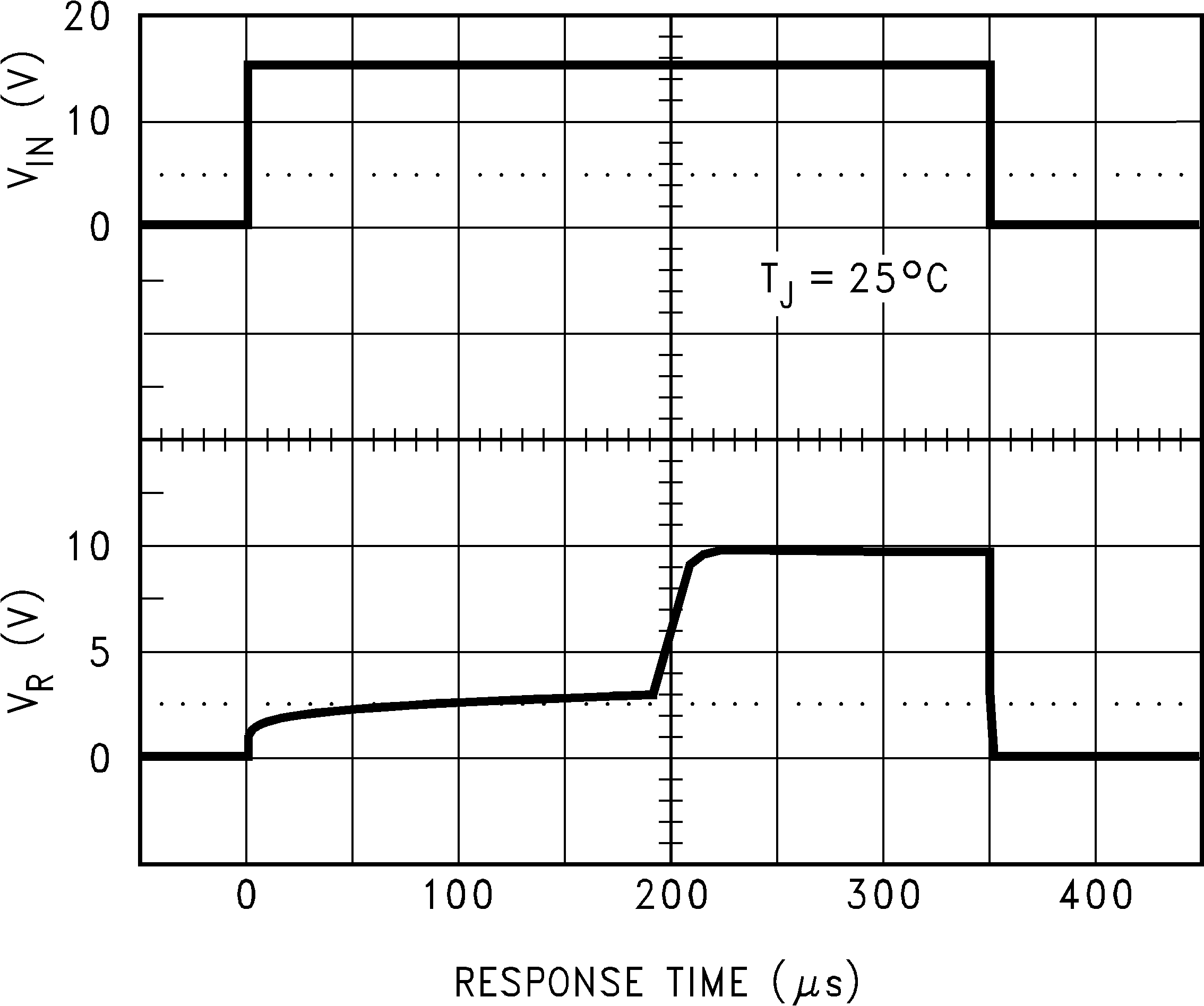
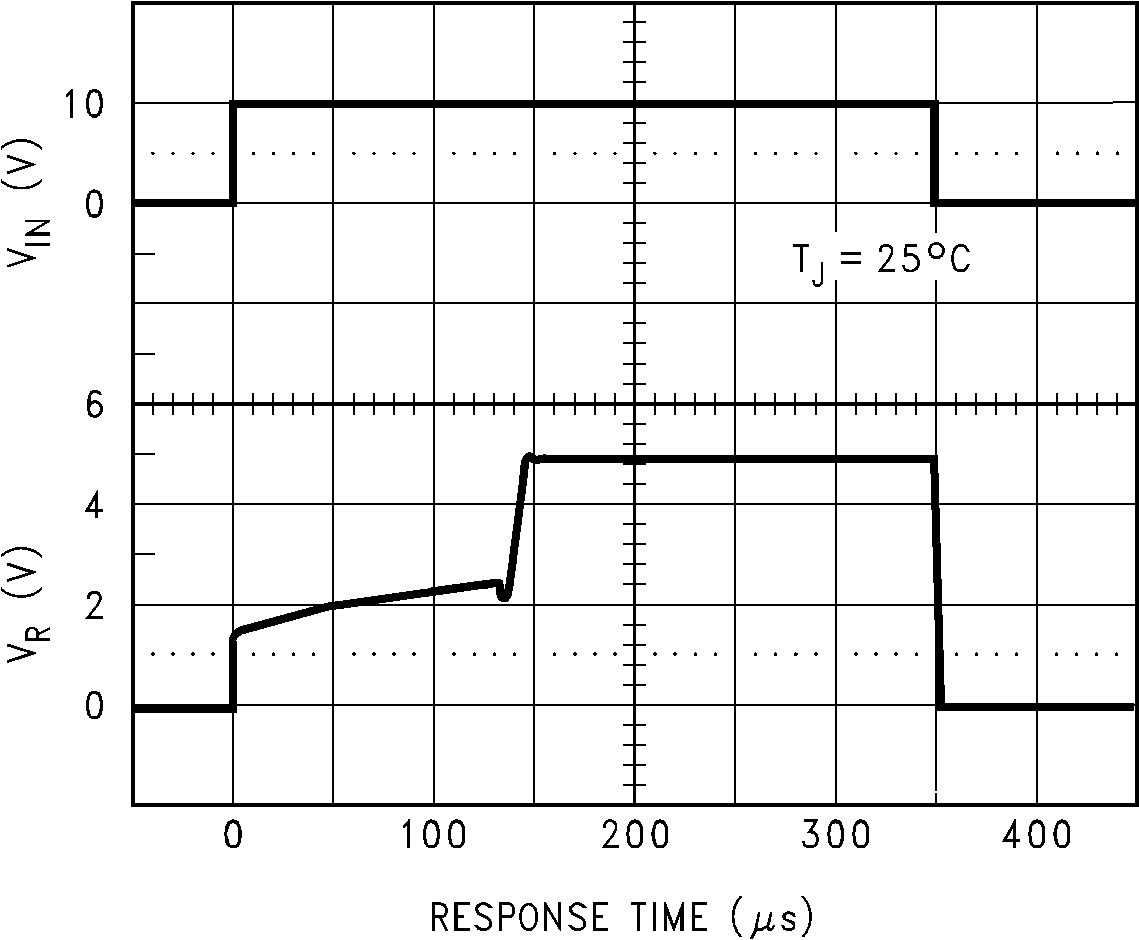
6.11.1 Start-Up Characteristics
