SNVS049F February 2000 – March 2016 LM4120
PRODUCTION DATA.
8 Application and Implementation
NOTE
Information in the following applications sections is not part of the TI component specification, and TI does not warrant its accuracy or completeness. TI’s customers are responsible for determining suitability of components for their purposes. Customers should validate and test their design implementation to confirm system functionality.
8.1 Application Information
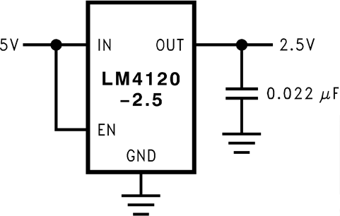
The standard application circuit for the LM4120 is shown in Figure 29. The device is designed to be stable with ceramic output capacitors in the range of 0.022 µF to 0.047 µF. The minimum required output capacitor is
0.022 µF. These capacitors typically have an ESR of about 0.1 Ω to 0.5 Ω. Smaller ESR can be tolerated, but larger ESR cannot be tolerated. The output capacitor can be increased to improve load transient response, up to about 1 µF. However, values above 0.047 µF must be tantalum. With tantalum capacitors in the 1-µF range, a small capacitor between the output and the reference pin is required. This capacitor will typically be in the 50-pF range. Care must be taken when using output capacitors of 1 µF or larger. These applications must be thoroughly tested over temperature, line, and load.
An input capacitor is typically not required. However, a 0.1-µF ceramic can be used to help prevent line transients from entering the LM4120. Larger input capacitors must be tantalum or aluminum.
The reference pin is sensitive to noise, and capacitive loading. Therefore, the PCB layout must isolate this pin as much as possible.
The enable pin is an analog input with very little hysteresis. About 6 µA into this pin is required to turn the part on, and it must be taken close to GND to turn the part off (see Electrical Characteristics for thresholds). If the shutdown feature is not required, then this pin can safely be connected directly to the input supply.
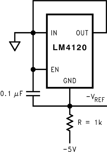 Figure 19. Voltage Reference With Negative Output Circuit
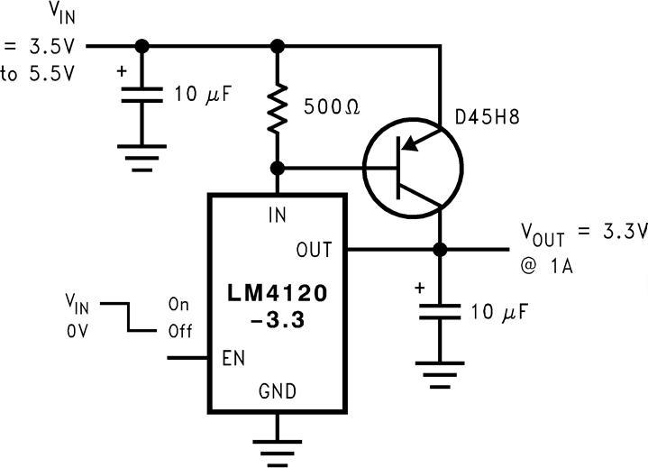 Figure 20. Precision High-Current Low-Dropout Regulator Circuit
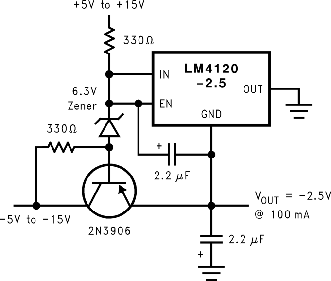 Figure 21. Precision High-Current Negative Voltage Regulator Circuit
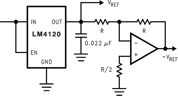 Figure 22. Voltage Reference With Complimentary Output Circuit
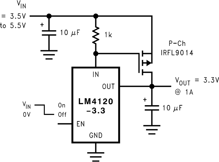 Figure 23. Precision High-Current Low-Dropout Regulator Circuit
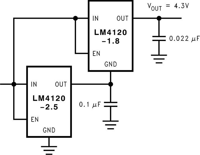 Figure 24. Stacking Voltage References Circuit
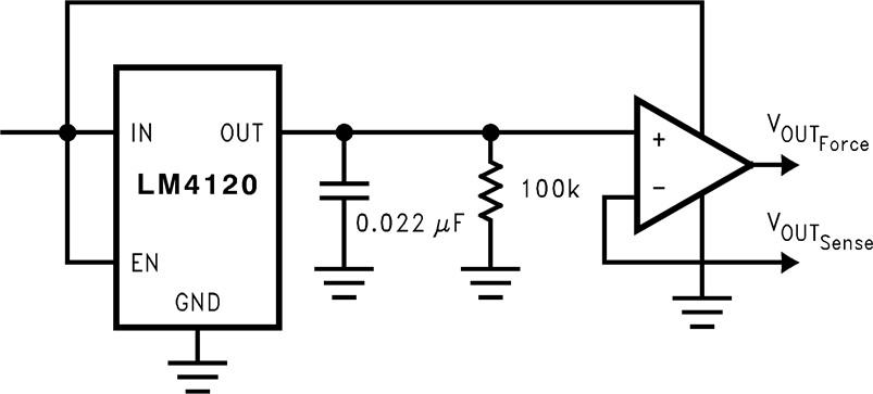 Figure 25. Precision Voltage Reference With Force and Sense Output Circuit
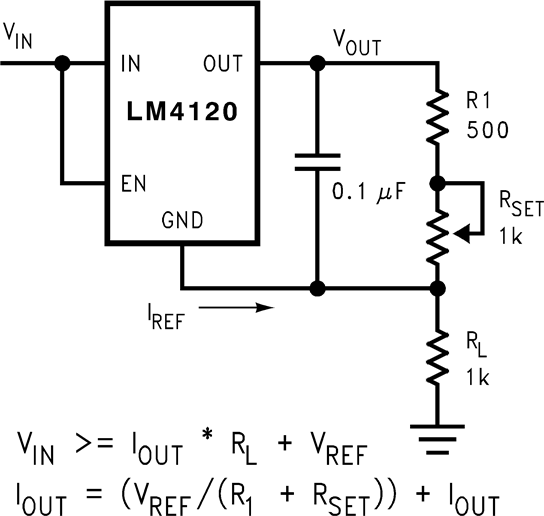 Figure 26. Programmable Current Source Circuit
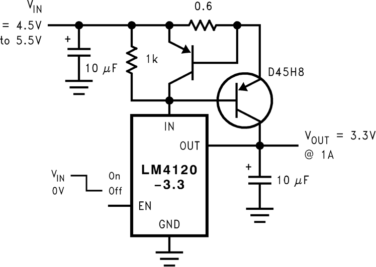 Figure 27. Precision Regulator With Current Limiting Circuit
8.2 Typical Application
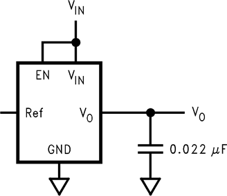 Figure 29. Standard Application Circuit
8.2.1 Design Requirements
For this design example, use the parameters listed in Table 2 as the input parameters.
Table 2. Design Parameters
| PARAMETER | EXAMPLE VALUE |
|---|---|
| Output Voltage VOUT | 1.8 V, 2.048 V, 2.5 V, 3 V, 3.3 V, 4.096 V, 5 V |
| Input Voltage Range VIN | VOUT 120 mV to 12 V |
| Load Current | 1 mA (typical) |
8.2.2 Detailed Design Procedure
8.2.2.1 Input Capacitors
Although not always required, an input capacitor is recommended. A supply bypass capacitor on the input assures that the reference is working from a source with low impedance, which improves stability. A bypass capacitor can also improve transient response by providing a reservoir of stored energy that the reference can utilize in case where the load current demand suddenly increases. The value used for CIN may be used without limit.
8.2.2.2 Output Capacitors
The LM4120 may require a 0.022-μF to 1-μF output capacitor for loop stability (compensation) as well as transient response. During the sudden changes in load current demand, the output capacitor must source or sink current during the time it takes the control loop of the LM4120 to respond.
8.2.3 Application Curves
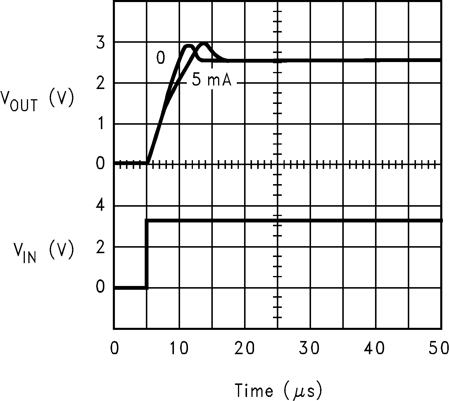 Figure 30. Start-Up Response
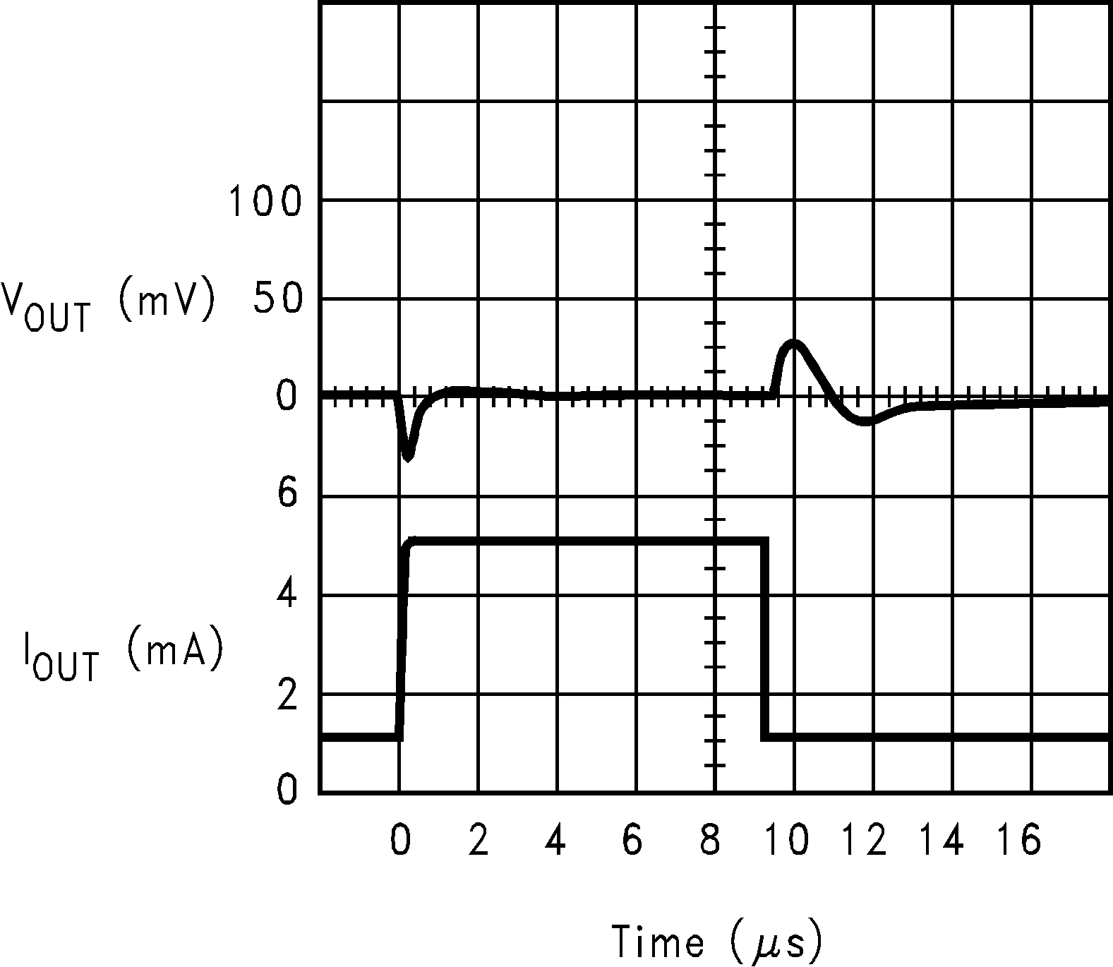 Figure 31. Load Step Response
