SNVS372G August   2005  – October 2016 LM4132 , LM4132-Q1

PRODUCTION DATA.  

  1. Features
  2. Applications
  3. Description
  4. Revision History
  5. Pin Configuration and Functions
  6. Specifications
    1. 6.1  Absolute Maximum Ratings
    2. 6.2  ESD Ratings
    3. 6.3  Recommended Operating Conditions
    4. 6.4  Thermal Information
    5. 6.5  Electrical Characteristics LM4132-1.8 (VOUT = 1.8 V)
    6. 6.6  Electrical Characteristics LM4132-2 (VOUT = 2.048 V)
    7. 6.7  Electrical Characteristics LM4132-2.5 (VOUT = 2.5 V)
    8. 6.8  Electrical Characteristics LM4132-3 (VOUT = 3 V)
    9. 6.9  Electrical Characteristics LM4132-3.3 (VOUT = 3.3 V)
    10. 6.10 Electrical Characteristics LM4132-3.3-Q1(VOUT = 3.3 V)
    11. 6.11 Electrical Characteristics LM4132-4.1 (VOUT = 4.096 V)
    12. 6.12 Typical Characteristics
      1. 6.12.1 Typical Characteristics for 1.8 V
      2. 6.12.2 Typical Characteristics for 2.048 V
      3. 6.12.3 Typical Characteristics for 2.5 V
      4. 6.12.4 Typical Characteristics for 3 V
      5. 6.12.5 Typical Characteristics for 3.3 V
      6. 6.12.6 Typical Characteristics for 4.096 V
  7. Detailed Description
    1. 7.1 Overview
    2. 7.2 Functional Block Diagram
    3. 7.3 Feature Description
      1. 7.3.1 Short Circuited Output
      2. 7.3.2 Turnon Time
      3. 7.3.3 Thermal Hysteresis
    4. 7.4 Device Functional Modes
  8. Applications and Implementation
    1. 8.1 Application Information
    2. 8.2 Typical Applications
      1. 8.2.1 LM4132 Typical Application
        1. 8.2.1.1 Design Requirements
        2. 8.2.1.2 Detailed Design Procedure
          1. 8.2.1.2.1 Supply and Enable Voltages
          2. 8.2.1.2.2 Component Selection
          3. 8.2.1.2.3 Temperature Coefficient
          4. 8.2.1.2.4 Long-Term Stability
          5. 8.2.1.2.5 Expression of Electrical Characteristics
        3. 8.2.1.3 Application Curves
      2. 8.2.2 Other Application Circuits
  9. Power Supply Recommendations
  10. 10Layout
    1. 10.1 Layout Guidelines
    2. 10.2 Layout Example
  11. 11Device and Documentation Support
    1. 11.1 Documentation Support
      1. 11.1.1 Related Documentation
    2. 11.2 Related Links
    3. 11.3 Receiving Notification of Documentation Updates
    4. 11.4 Community Resources
    5. 11.5 Trademarks
    6. 11.6 Electrostatic Discharge Caution
    7. 11.7 Glossary
  12. 12Mechanical, Packaging, and Orderable Information

封装选项

机械数据 (封装 | 引脚)
散热焊盘机械数据 (封装 | 引脚)
订购信息

5 Pin Configuration and Functions

DBV Package
5-Pin SOT-23
Top View
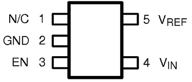
LM4132 LM4132-Q1 20151302.gif

Pin Functions

PIN I/O(1) DESCRIPTION
NO. NAME
1 N/C No connect pin, leave floating
2 GND G Ground
3 EN I Enable pin
4 VIN P Input supply
5 VREF P Reference output
(1) G: Ground; I: Input; P: Power