SNVS053F June 2000 – September 2016 LM4140
PRODUCTION DATA.
- 1 Features
- 2 Applications
- 3 Description
- 4 Revision History
- 5 Pin Configuration and Functions
- 6 Specifications
- 7 Detailed Description
-
8 Application and Implementation
- 8.1 Application Information
- 8.2
Typical Applications
- 8.2.1 Precision DAC Reference
- 8.2.2 Boosted Output Current
- 8.2.3 Boosted Output Current With Current Limiter
- 8.2.4 Complimentary Outputs
- 8.2.5 Voltage Reference With Force and Sense Output
- 8.2.6 Precision Programmable Current Source
- 8.2.7 Strain Gauge Conditioner for 350-Ω Bridge
- 8.2.8 Bipolar Voltage References for Low Power ADC
- 8.2.9 Self-Biased Low Power ADC Reference With Trim Current Sources
- 9 Power Supply Recommendations
- 10Layout
- 11Device and Documentation Support
- 12Mechanical, Packaging, and Orderable Information
8 Application and Implementation
NOTE
Information in the following applications sections is not part of the TI component specification, and TI does not warrant its accuracy or completeness. TI’s customers are responsible for determining suitability of components for their purposes. Customers should validate and test their design implementation to confirm system functionality.
8.1 Application Information
8.1.1 Input Capacitors
Although not always required, TI recommends an input capacitor. A supply bypass capacitor on the input assures that the reference is working from a source with low impedance, which improves stability. A bypass capacitor can also improve transient response by providing a reservoir of stored energy that the reference can use in case where the load current demand suddenly increases. The value used for CIN may be used without limit.
8.1.2 Output Capacitors
The LM4140 requires a 1-µF (nominally) output capacitor for loop stability (compensation) as well as transient response. During the sudden changes in load current demand, the output capacitor must source or sink current during the time it takes the control loop of the LM4140 to respond.
This capacitor must be selected to meet the requirements of minimum capacitance and equivalent series resistance (ESR) range.
In general, the capacitor value must be at least 0.2 µF (over the actual ambient operating temperature), and the ESR must be within the range indicated in Figure 22, Figure 23, and Figure 24.
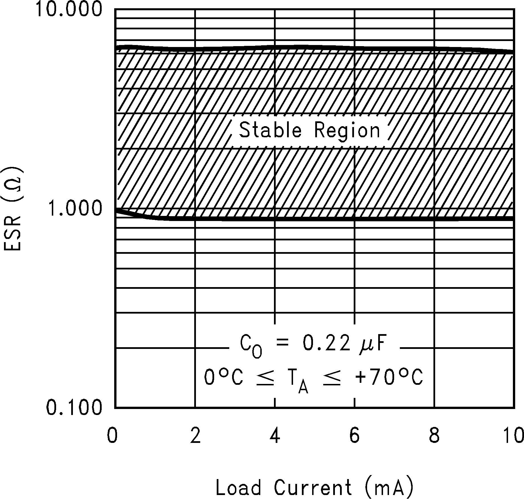 Figure 22. 0.22-µF ESR Range
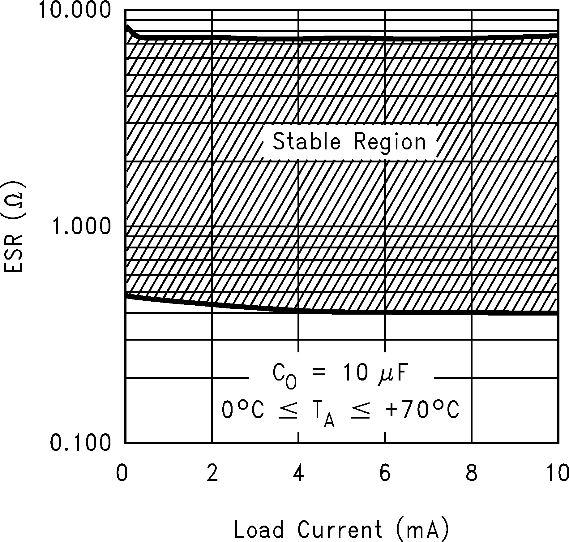 Figure 24. 10-µF ESR Range
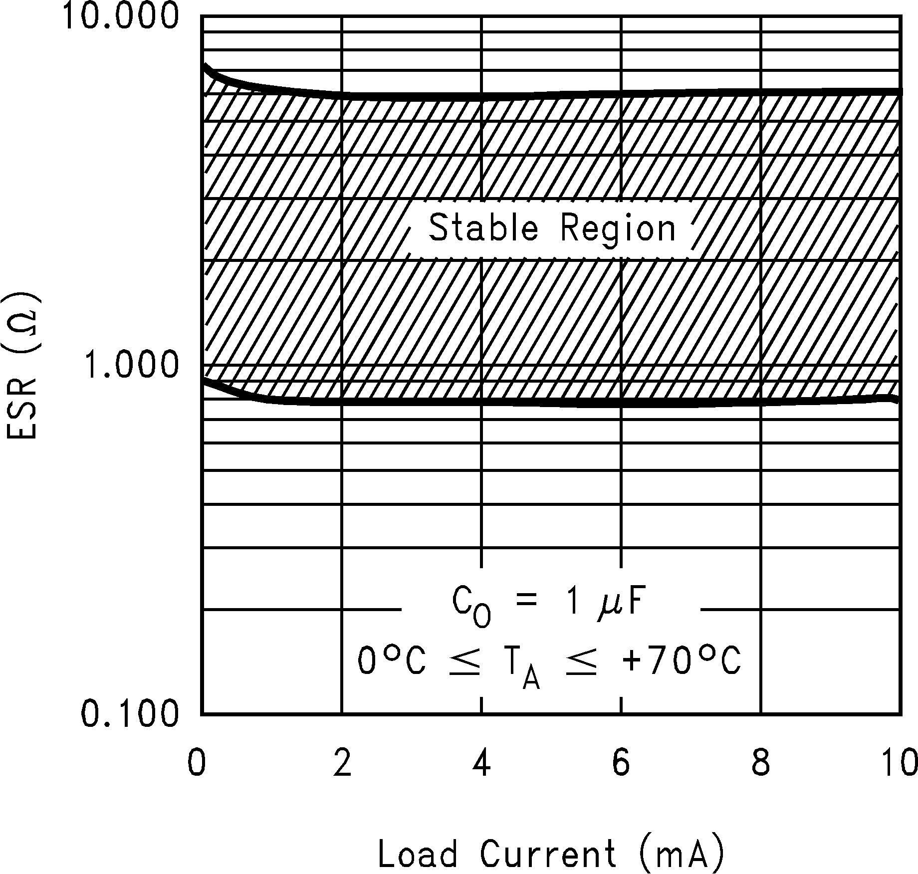 Figure 23. 1-µF ESR Range
8.1.3 Tantalum Capacitors
Surface-mountable solid tantalum capacitors offer a good combination of small physical size for the capacitance value, and ESR in the range required by the LM4140. The results of testing the LM4140 stability with surface mount solid tantalum capacitors show good stability with values in the range of 0.1 µF. However, optimum performance is achieved with a 1-µF capacitor.
Table 2 shows tantalum capacitors that have been verified as suitable for use with the LM4140.
Table 2. 1-µF Surface-Mount Tantalum Capacitor Selection Guide
| MANUFACTURER | PART NUMBER |
|---|---|
| Kemet | T491A105M010AS |
| NEC | NRU105N10 |
| Siemens | B45196-E3105-K |
| Nichicon | F931C105MA |
| Sprague | 293D105X0016A2T |
Table 3. 2.2-µF Surface-Mount Tantalum Capacitor Selection Guide
| MANUFACTURER | PART NUMBER |
|---|---|
| Kemet | T491A225M010AS |
| NEC | NRU225M06 |
| Siemens | B45196/2.2/10/10 |
| Nichicon | F930J225MA |
| Sprague | 293D225X0010A2T |
8.1.4 Aluminum Electrolytic Capacitors
Although probably not a good choice for a production design, because of relatively large physical size, an aluminium electrolytic capacitor can be used in the design prototype for an LM4140 reference. A 1-µF capacitor meeting the ESR conditions can be used. If the operating temperature drops below 0°C, the reference may not remain stable, as the ESR of the aluminium electrolytic capacitor increases, and may exceed the limits indicated in the figures.
8.1.5 Multilayer Ceramic Capacitors
Surface-mountable multilayer ceramic capacitors may be an attractive choice because of their relatively small physical size and excellent RF characteristics.
However, they sometimes have an ESR values lower than the minimum required by the LM4140, and relatively large capacitance change with temperature. The manufacturer's datasheet for the capacitor must be consulted before selecting a value. Test results of LM4140 stability using multilayer ceramic capacitors show that a minimum of 0.2 µF is usually required.
Table 4 shows the multilayer ceramic capacitors that have been verified as suitable for use with the LM4140.
Table 4. Surface-Mount Ceramic Capacitors Selection Guide
| CAPACITOR (µF) | MANUFACTURER | PART NUMBER |
|---|---|---|
| 2.2 | Tokin | 1E225ZY5U-C203 |
| 2.2 | Murata | GRM42-6Y5V225Z16 |
| 4.7 | Tokin | 1E475ZY5U-C304 |
8.1.6 Reverse Current Path
The P-channel Pass transistor used in the LM4140 has an inherent diode connected between the VIN and VREF pins (see Figure 25).
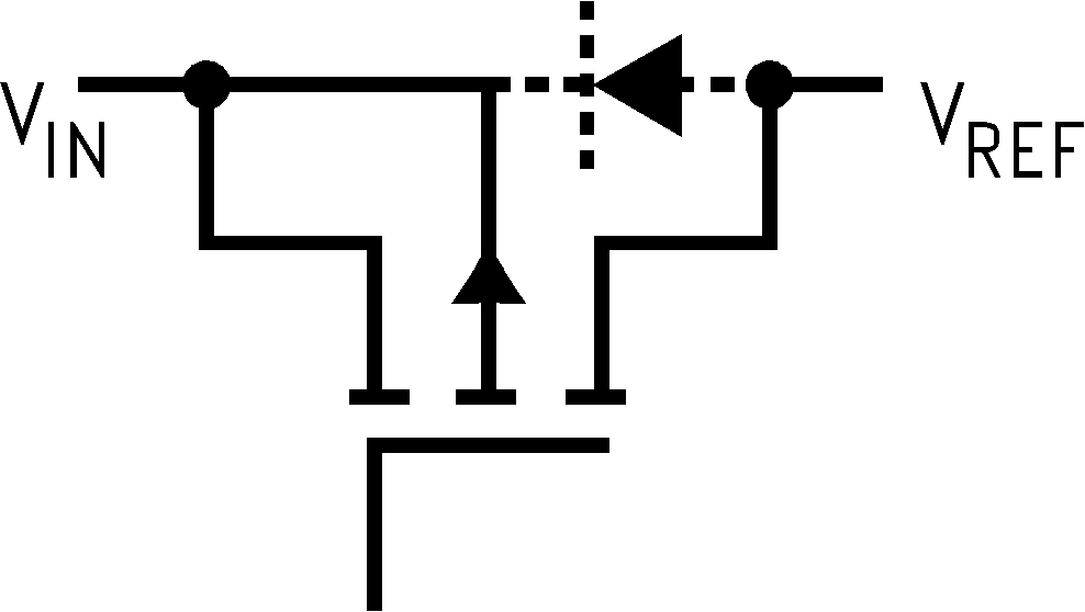 Figure 25. Internal P-Channel Pass Transistor
Forcing the output to voltages higher than the input, or pulling VIN below voltage stored on the output capacitor by more than a Vbe, forward biases this diode and current flows from the VREF terminal to VIN. No damage to the LM4140 occurs under these conditions as long as the current flowing into the output pin does not exceed 50 mA.
8.1.7 Output Accuracy
Like all references, either series or shunt, the after assembly accuracy is made up of primarily three components: initial accuracy itself, thermal hysteresis, and effects of the PCB assembly stress.
LM4140 provides an excellent output initial accuracy of 0.1% and temperature coefficient of 6ppm/°C (B Grade).
For best accuracy and precision, the LM4140 junction temperature must not exceed 70°C.
The thermal hysteresis curve on this datasheet are performance characteristics of three typical parts selected at random from a sample of 40 parts.
Parts are mounted in a socket to minimize the effect of PCB's mechnical expansion and contraction. Readings are taken at 25°C following multiple temperature cycles to 0°C and 70°C. The labels on the X axis of Figure 26 indicate the device temperature cycle prior to measurement at 25°C.
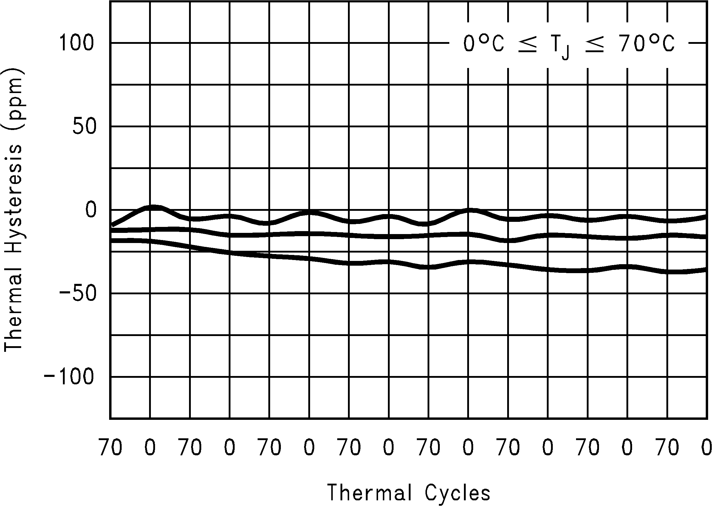 Figure 26. Typical Thermal Hysteresis
The mechanical stress due to the PCB's mechanical and thermal stress can cause an output voltage shift more than the true thermal coefficient of the device. References in surface mount packages are more susceptible to these stresses because of the small amount of plastic molding which support the leads.
Following the recommendations on Layout can minimize the mechanical stress on the device.
8.2 Typical Applications
8.2.1 Precision DAC Reference
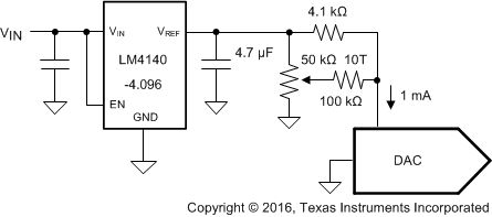 Figure 27. Precision DAC Reference Schematic
8.2.1.1 Design Requirements
Generate a precision, temperature-stable voltage reference for use in digital-to-analog converter applications.
8.2.1.2 Detailed Design Procedure
Use LM4140-4.096 to generate a 4.096-V reference voltage. Use an adjustable resistor network to fine tune the reference.
8.2.1.3 Application Curves
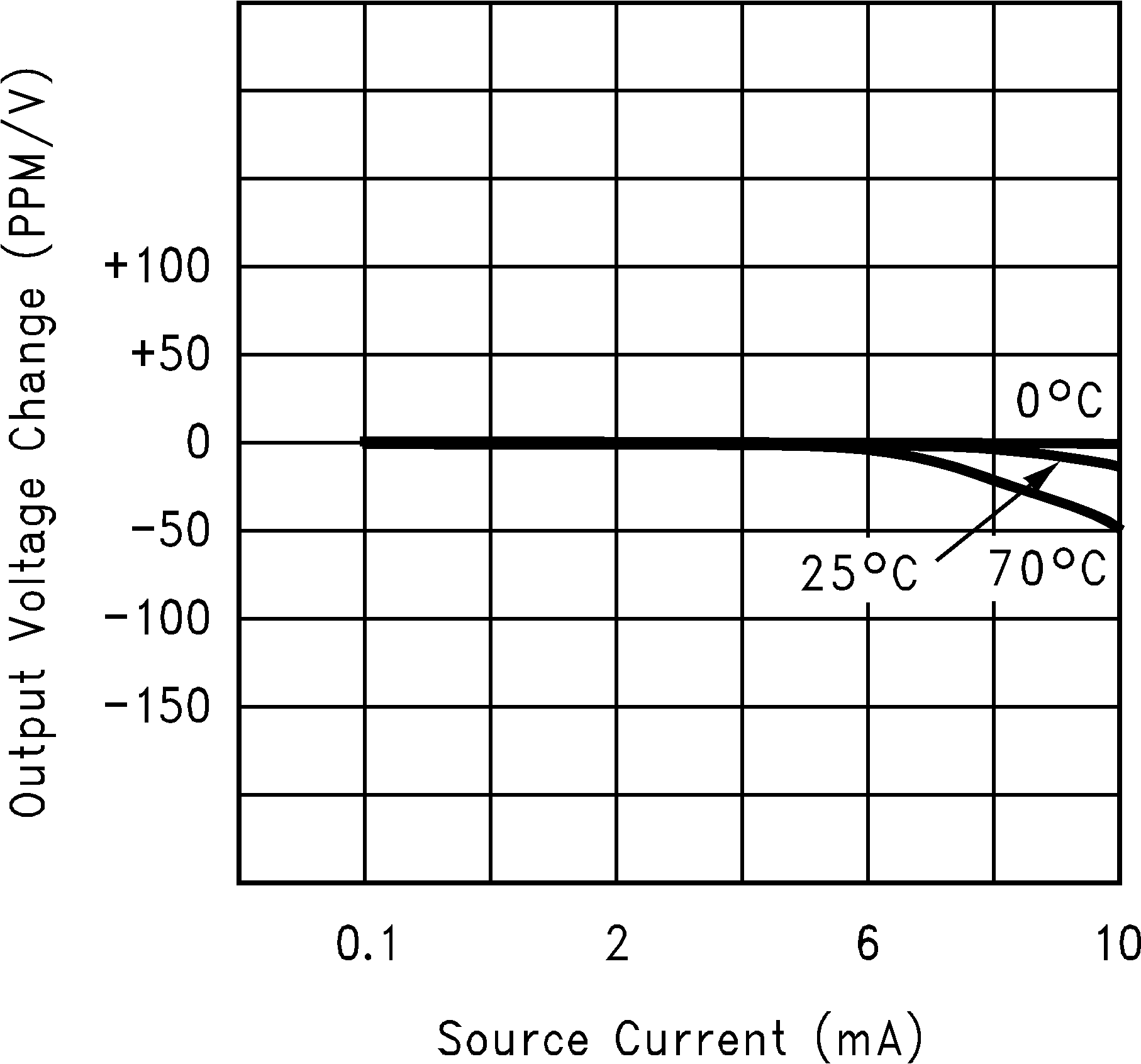 Figure 28. Output Voltage vs Load Current
 Figure 29. Typical Temperature Coefficient
(Sample of 5 Parts)
8.2.2 Boosted Output Current
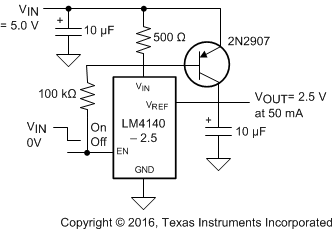 Figure 30. Boosted Output Current Schematic
8.2.2.1 Design Requirements
Generate a reference voltage that can support 50 mA.
8.2.2.2 Detailed Design Procedure
The LM4140-2.5 sets the reference level at 2.5 V. A 2N2907 PNP transistor is added, where the base is tied to VIN through a 500-Ω resistor. The input current into the LM4140 increases with load current, which increases the voltage drop across the 500-Ω resistor until the PNP transistor turns on and supplements the load current. See Figure 30 for the circuit diagram.
8.2.3 Boosted Output Current With Current Limiter
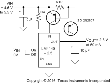 Figure 31. Boosted Output Current With Current Limiter Schematic
8.2.3.1 Design Requirements
Generate a reference voltage that can support 50 mA with current limiter.
8.2.3.2 Detailed Design Procedure
The LM4140-2.5 sets the reference level at 2.5 V. Similar to Boosted Output Current, a PNP transistor is added between VIN and the output. Another PNP transistor is added to sense the current between VIN and the load. This additional transistor turns on above 50 mA, which turns off the pass transistor to the load.
8.2.4 Complimentary Outputs
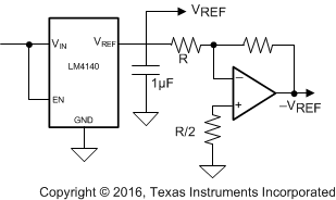
8.2.4.1 Design Requirements
Generate a positive and negative voltage reference.
8.2.4.2 Detailed Design Procedure
Use the LM4140 to generate the positive reference. Pass the reference into a unity gain inverting amplifier for a negative reference output.
8.2.5 Voltage Reference With Force and Sense Output
 Figure 33. Voltage Reference With Force and Sense Output Schematic
8.2.5.1 Design Requirements
Design a voltage reference source that has a force and sense output.
8.2.5.2 Detailed Design Procedure
Use the LM4140 to generate a reference voltage. Pass this into the positive input terminal of an operation amplifier, and use the negative input as the sense input from the load.
8.2.6 Precision Programmable Current Source
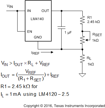 Figure 34. Precision Programmable Current Source Schematic
8.2.6.1 Design Requirements
Create a precision, adjustable current source.
8.2.6.2 Detailed Design Procedure
Use LM4140 to create reference voltage across an adjustable resistor, R1 + RSET. The voltage reference creates a constant voltage source, and the adjustable resistor generates a proportional current.
8.2.7 Strain Gauge Conditioner for 350-Ω Bridge
 Figure 35. Strain Gauge Conditioner for 350-Ω Bridge Schematic
8.2.7.1 Design Requirements
Supply a strain gage with a precision reference voltage.
8.2.7.2 Detailed Design Procedure
Use LM4140 to generate 4.096-V reference voltage. Use the reference to drive the strain gage bridge.
8.2.8 Bipolar Voltage References for Low Power ADC
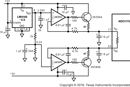 Figure 36. Bipolar Voltage References for Low Power ADC Schematic
8.2.8.1 Design Requirements
Provide positive and negative reference voltages for the ADC1175 low power ADC.
8.2.8.2 Detailed Design Procedure
Use LM4140 to generate a 2.5-V positive reference voltage. The reference voltage is passed into an opamp to act as a buffer and inverter, which yields a positive and negative reference. Transistors are used to drive the low impedance inputs of the ADC1175.
8.2.9 Self-Biased Low Power ADC Reference With Trim Current Sources
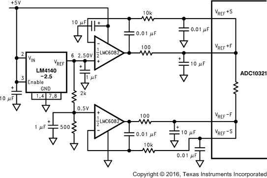 Figure 37. Self-Biased Low Power ADC Reference With Trim Current Sources Schematic
8.2.9.1 Design Requirements
Use ADC1175 internal reference, but increase accuracy with trimming currents.
8.2.9.2 Detailed Design Procedure
The LM4140-2.5 sets a stable voltage source which is buffered and inverted, and the opamps are used as force and sense amplifiers. This application does not require the transistor to drive low impedance nodes as the internal reference voltages are still being used. The external circuitry is to increase the accuracy of the internal reference.