SNVS053F June 2000 – September 2016 LM4140
PRODUCTION DATA.
- 1 Features
- 2 Applications
- 3 Description
- 4 Revision History
- 5 Pin Configuration and Functions
- 6 Specifications
- 7 Detailed Description
-
8 Application and Implementation
- 8.1 Application Information
- 8.2
Typical Applications
- 8.2.1 Precision DAC Reference
- 8.2.2 Boosted Output Current
- 8.2.3 Boosted Output Current With Current Limiter
- 8.2.4 Complimentary Outputs
- 8.2.5 Voltage Reference With Force and Sense Output
- 8.2.6 Precision Programmable Current Source
- 8.2.7 Strain Gauge Conditioner for 350-Ω Bridge
- 8.2.8 Bipolar Voltage References for Low Power ADC
- 8.2.9 Self-Biased Low Power ADC Reference With Trim Current Sources
- 9 Power Supply Recommendations
- 10Layout
- 11Device and Documentation Support
- 12Mechanical, Packaging, and Orderable Information
7 Detailed Description
7.1 Overview
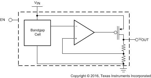
The LM4140 device is a high-precision series voltage reference available in 5 difference output voltage options, including the 1.024-V option below the bandgap voltage. The series reference can operate with input voltage as low as VREF + 400 mV over temperature, consuming 400 µA or less over temperature depending on voltage option. While in shutdown, the device consumes 10 nA (typical).
7.2 Functional Block Diagram

7.3 Feature Description
7.3.1 ON/OFF Operation
The LM4140 is designed to quickly reduce both VREF and IQ to zero when turned off. VREF is restored in less than 200 µs when turned on. During the turnoff, the charge across the output capacitor is discharged to ground through internal circuitry.
The LM4140 is turned off by pulling the enable input low, and turned on by driving the input high. If this feature is not to be used, the enable pin must be tied to the VIN to keep the reference on at all times (the enable pin must not be left floating).
To ensure proper operation, the signal source used to drive the enable pin must be able to swing above and below the specified high and low voltage thresholds which ensure an ON or OFF state (see Electrical Characteristics).
The ON/OFF signal may come from either a totem-pole output, or an open-collector output with pullup resistor to the LM4140 input voltage. This high-level voltage may exceed the LM4140 input voltage, but must remain within the absolute maximum rating for the enable pin.
7.4 Device Functional Modes
Table 1 lists the operational modes of the LM4140.
Table 1. Operational Modes
| ENABLE PIN | LOGIC STATE | DESCRIPTION |
|---|---|---|
| EN = VIN | 1 | Normal operation, device powered up |
| EN = Ground | 0 | Device in shutdown |