SNVS053F June   2000  – September 2016 LM4140

PRODUCTION DATA.  

  1. Features
  2. Applications
  3. Description
  4. Revision History
  5. Pin Configuration and Functions
  6. Specifications
    1. 6.1 Absolute Maximum Ratings
    2. 6.2 ESD Ratings
    3. 6.3 Recommended Operating Conditions
    4. 6.4 Thermal Information
    5. 6.5 Electrical Characteristics
    6. 6.6 Typical Characteristics
  7. Detailed Description
    1. 7.1 Overview
    2. 7.2 Functional Block Diagram
    3. 7.3 Feature Description
      1. 7.3.1 ON/OFF Operation
    4. 7.4 Device Functional Modes
  8. Application and Implementation
    1. 8.1 Application Information
      1. 8.1.1 Input Capacitors
      2. 8.1.2 Output Capacitors
      3. 8.1.3 Tantalum Capacitors
      4. 8.1.4 Aluminum Electrolytic Capacitors
      5. 8.1.5 Multilayer Ceramic Capacitors
      6. 8.1.6 Reverse Current Path
      7. 8.1.7 Output Accuracy
    2. 8.2 Typical Applications
      1. 8.2.1 Precision DAC Reference
        1. 8.2.1.1 Design Requirements
        2. 8.2.1.2 Detailed Design Procedure
        3. 8.2.1.3 Application Curves
      2. 8.2.2 Boosted Output Current
        1. 8.2.2.1 Design Requirements
        2. 8.2.2.2 Detailed Design Procedure
      3. 8.2.3 Boosted Output Current With Current Limiter
        1. 8.2.3.1 Design Requirements
        2. 8.2.3.2 Detailed Design Procedure
      4. 8.2.4 Complimentary Outputs
        1. 8.2.4.1 Design Requirements
        2. 8.2.4.2 Detailed Design Procedure
      5. 8.2.5 Voltage Reference With Force and Sense Output
        1. 8.2.5.1 Design Requirements
        2. 8.2.5.2 Detailed Design Procedure
      6. 8.2.6 Precision Programmable Current Source
        1. 8.2.6.1 Design Requirements
        2. 8.2.6.2 Detailed Design Procedure
      7. 8.2.7 Strain Gauge Conditioner for 350-Ω Bridge
        1. 8.2.7.1 Design Requirements
        2. 8.2.7.2 Detailed Design Procedure
      8. 8.2.8 Bipolar Voltage References for Low Power ADC
        1. 8.2.8.1 Design Requirements
        2. 8.2.8.2 Detailed Design Procedure
      9. 8.2.9 Self-Biased Low Power ADC Reference With Trim Current Sources
        1. 8.2.9.1 Design Requirements
        2. 8.2.9.2 Detailed Design Procedure
  9. Power Supply Recommendations
  10. 10Layout
    1. 10.1 Layout Guidelines
    2. 10.2 Layout Example
  11. 11Device and Documentation Support
    1. 11.1 Receiving Notification of Documentation Updates
    2. 11.2 Community Resources
    3. 11.3 Trademarks
    4. 11.4 Electrostatic Discharge Caution
    5. 11.5 Glossary
  12. 12Mechanical, Packaging, and Orderable Information

封装选项

机械数据 (封装 | 引脚)
散热焊盘机械数据 (封装 | 引脚)
订购信息

10 Layout

10.1 Layout Guidelines

The simplest ways to reduce the stress related shifts are:

  1. Mounting the device near the edges or the corners of the board where mechanical stress is at its minimum. The center of the board generally has the highest mechanical and thermal expansion stress.
  2. Mechanical isolation of the device by creating an island by cutting a U shape slot on the PCB for mounting the device. This approach would also provide some thermal isolation from the rest of the circuit.

Figure 39 is a recommended printed-circuit board layout with a slot cut on three sides of the circuit layout to serve as a strain relief.

10.2 Layout Example

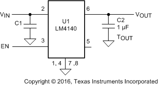
LM4140 10107934.png Figure 38. Suggested Schematic and External Components
LM4140 10107935.gif Figure 39. Suggested PCB Layout With Slot