SNVS020H May 2000 – January 2016 LM431
PRODUCTION DATA.
- 1 Features
- 2 Applications
- 3 Description
- 4 Revision History
- 5 Pin Configuration and Functions
- 6 Specifications
- 7 Parameter Measurement Information
- 8 Detailed Description
- 9 Application and Implementation
- 10Power Supply Recommendations
- 11Layout
- 12Device and Documentation Support
- 13Mechanical, Packaging, and Orderable Information
封装选项
机械数据 (封装 | 引脚)
散热焊盘机械数据 (封装 | 引脚)
订购信息
6 Specifications
6.1 Absolute Maximum Ratings
over operating free-air temperature range (unless otherwise noted)(1)(2)| MIN | MAX | UNIT | ||
|---|---|---|---|---|
| Cathode voltage | 37 | V | ||
| Reference voltage | –0.5 | V | ||
| Continuous cathode current | –10 | 150 | mA | |
| Reference input current | 10 | mA | ||
| Internal power dissipation(3)(4) | TO-92 package | 0.78 | W | |
| SOIC package | 0.81 | W | ||
| SOT-23 package | 0.28 | W | ||
| Operating temperature | Industrial (LM431xI) | –40 | 85 | °C |
| Commercial (LM431xC) | 0 | 70 | °C | |
| Storage temperature | –65 | 150 | °C | |
(1) Stresses beyond those listed under Absolute Maximum Ratings may cause permanent damage to the device. These are stress ratings only, which do not imply functional operation of the device at these or any other conditions beyond those indicated under Recommended Operating Conditions. Exposure to absolute-maximum-rated conditions for extended periods may affect device reliability.
(2) If Military/Aerospace specified devices are required, please contact the TI Sales Office/ Distributors for availability and specifications.
(3) TJ Max = 150°C.
(4) Ratings apply to ambient temperature at 25°C. Above this temperature, derate the TO-92 at 6.2 mW/°C, the SOIC at 6.5 mW/°C, the SOT-23 at 2.2 mW/°C.
6.2 ESD Ratings
| VALUE | UNIT | |||
|---|---|---|---|---|
| V(ESD) | Electrostatic discharge | Human-body model (HBM), per ANSI/ESDA/JEDEC JS-001(1) | ±2500 | V |
(1) JEDEC document JEP155 states that 500-V HBM allows safe manufacturing with a standard ESD control process.
6.3 Recommended Operating Conditions
over operating free-air temperature range (unless otherwise noted)| MIN | MAX | UNIT | |
|---|---|---|---|
| Cathode voltage | VREF | 37 | V |
| Cathode current | 1 | 100 | mA |
6.4 Thermal Information
| THERMAL METRIC(1) | LM431 | UNIT | |||
|---|---|---|---|---|---|
| D (SOIC) | DBZ (SOT-23) | LP (TO-92) | |||
| 8 PINS | 3 PINS | 3 PINS | |||
| RθJA | Junction-to-ambient thermal resistance | 126.9 | 267.7 | 162.4 | °C/W |
| RθJC(top) | Junction-to-case (top) thermal resistance | 72.2 | 138.3 | 85.8 | °C/W |
| RθJB | Junction-to-board thermal resistance | 67.5 | 61 | — | °C/W |
| ψJT | Junction-to-top characterization parameter | 21.1 | 21.5 | 29.4 | °C/W |
| ψJB | Junction-to-board characterization parameter | 67 | 60.1 | 141.5 | °C/W |
| RθJC(bot) | Junction-to-case (bottom) thermal resistance | — | — | — | °C/W |
(1) For more information about traditional and new thermal metrics, see the Semiconductor and IC Package Thermal Metrics application report, SPRA953.
6.5 Electrical Characteristics
TA = 25°C unless otherwise specified| PARAMETER | TEST CONDITIONS | MIN | TYP | MAX | UNIT | ||
|---|---|---|---|---|---|---|---|
| VREF | Reference voltage | VZ = VREF, II = 10 mA LM431A (Figure 6 ) |
2.44 | 2.495 | 2.55 | V | |
| VZ = VREF, II = 10 mA LM431B (Figure 6 ) |
2.47 | 2.495 | 2.52 | ||||
| VZ = VREF, II = 10 mA LM431C (Figure 6 ) |
2.485 | 2.5 | 2.51 | ||||
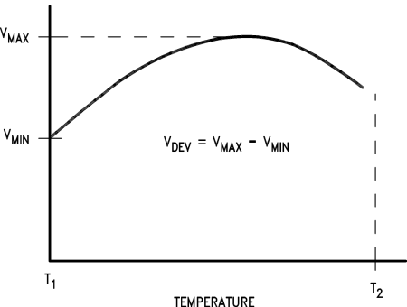
| VDEV | Deviation of reference input voltage overtemperature(1) | VZ = VREF, II = 10 mA, TA = full range (Figure 6 ) |
8 | 17 | mV | ||
| ΔVREF/ΔVZ | Ratio of the change in reference voltage to the change in cathode voltage | IZ = 10 mA (Figure 7 ) | VZ from VREF to 10 V | −1.4 | −2.7 | mV/V | |
| VZ from 10 V to 36 V | −1 | −2 | |||||
| IREF | Reference input current | R1 = 10 kΩ, R2 = ∞, II = 10 mA (Figure 7 ) | 2 | 4 | μA | ||
| ∝IREF | Deviation of reference input current overtemperature | R1 = 10 kΩ, R2 = ∞, II = 10 mA, TA = full range (Figure 7 ) |
0.4 | 1.2 | μA | ||
| IZ(MIN) | Minimum cathode current for regulation | VZ = VREF(Figure 6 ) | 0.4 | 1 | mA | ||
| IZ(OFF) | OFF-state current | VZ = 36 V, VREF = 0 V (Figure 8) | 0.3 | 1 | μA | ||
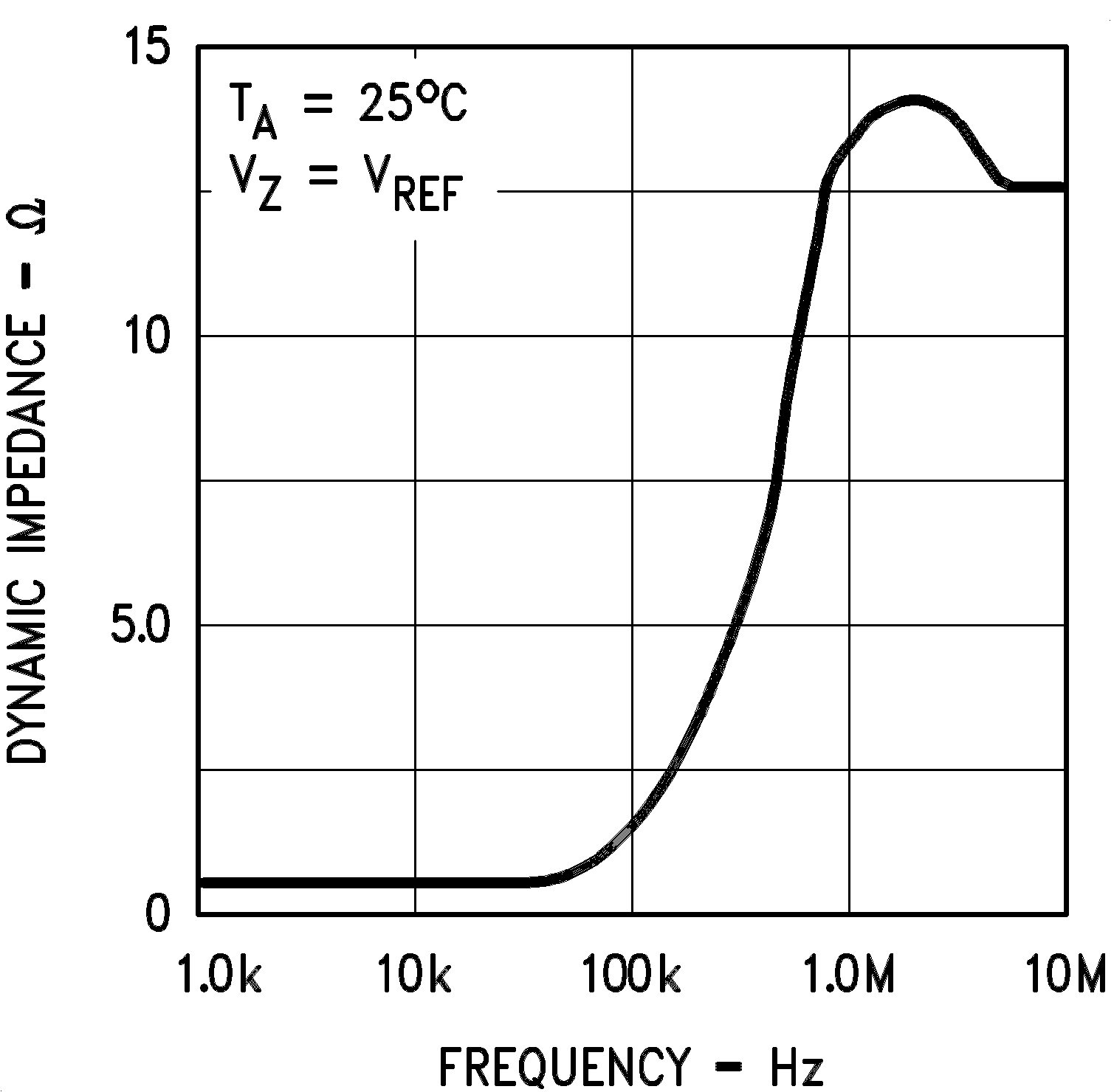
| rZ | Dynamic output impedance(2) | VZ = VREF, LM431A, Frequency = 0 Hz (Figure 6 ) |
0.75 | Ω | |||
| VZ = VREF, LM431B, LM431C Frequency = 0 Hz (Figure 6 ) |
0.5 | ||||||
(1) Deviation of reference input voltage, VDEV, is defined as the maximum variation of the reference input voltage over the full temperature range.

The average temperature coefficient of the reference input voltage, ∝VREF, is defined as:

Where:
T2 – T1 = full temperature change (0–70°C).
VREF can be positive or negative depending on whether the slope is positive or negative.
Example: VDEV = 8 mV, VREF = 2495 mV, T2 – T1 = 70°C, slope is positive.


The average temperature coefficient of the reference input voltage, ∝VREF, is defined as:

Where:
T2 – T1 = full temperature change (0–70°C).
VREF can be positive or negative depending on whether the slope is positive or negative.
Example: VDEV = 8 mV, VREF = 2495 mV, T2 – T1 = 70°C, slope is positive.

(2) The dynamic output impedance, rZ, is defined as:

When the device is programmed with two external resistors, R1 and R2, (see Figure 7), the dynamic output impedance of the overall circuit, rZ, is defined as:


When the device is programmed with two external resistors, R1 and R2, (see Figure 7), the dynamic output impedance of the overall circuit, rZ, is defined as:

6.6 Typical Characteristics


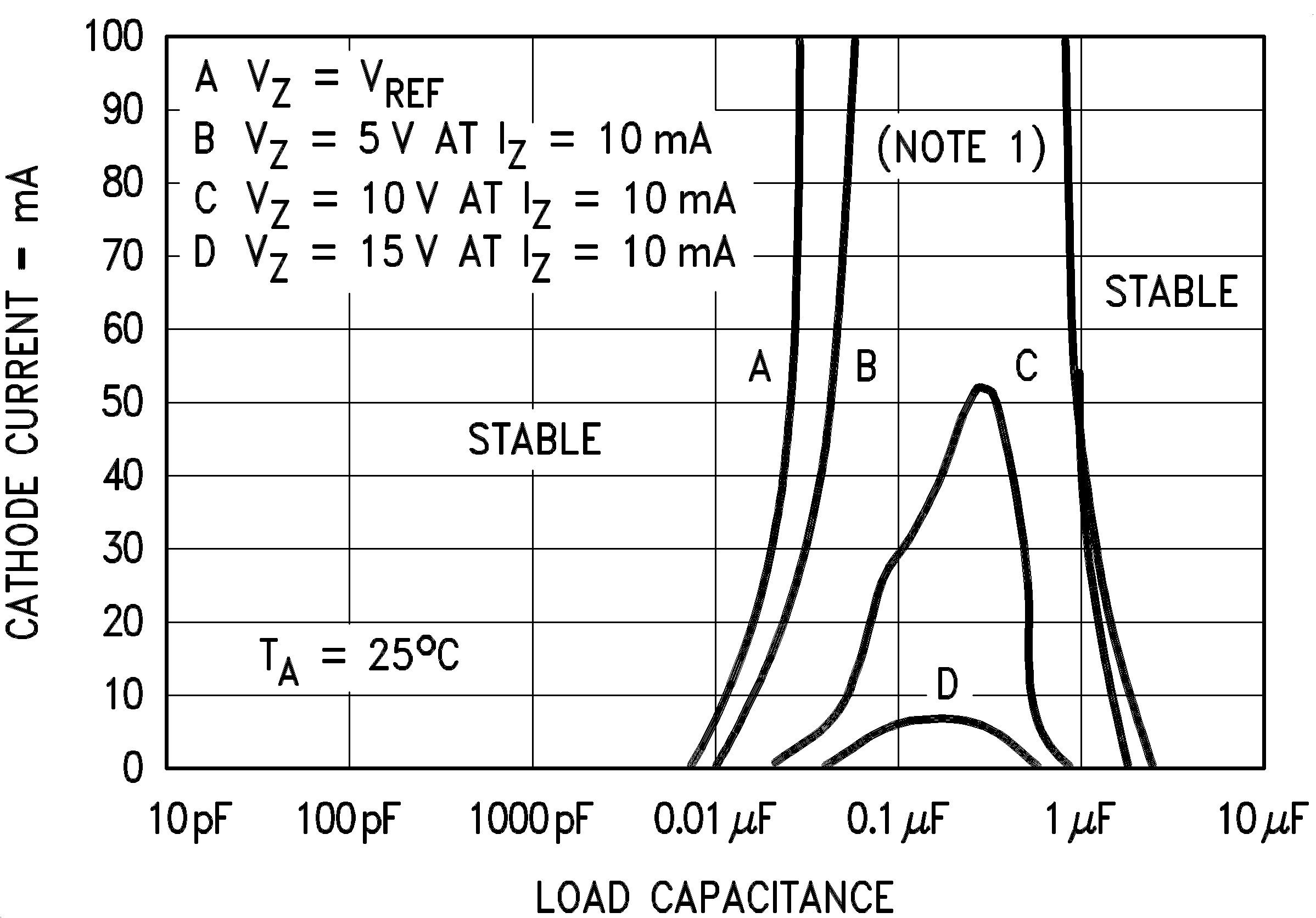
Note: The areas under the curves represent conditions that may cause the device to oscillate. For curves B, C, and D, R2 and V+ were adjusted to establish the initial VZ and IZ conditions with CL = 0. V+ and CL were then adjusted to determine the ranges of stability.
Figure 2. Stability Boundary Conditions