ZHCSCW5B August 2014 – September 2017 LM43600
PRODUCTION DATA.
- 1 特性
- 2 应用
- 3 说明
- 4 简化电路原理图
- 5 修订历史记录
- 6 Pin Configuration and Functions
- 7 Specifications
-
8 Detailed Description
- 8.1 Overview
- 8.2 Functional Block Diagram
- 8.3
Feature Description
- 8.3.1 Fixed Frequency Peak Current Mode Controlled Step-Down Regulator
- 8.3.2 Light Load Operation
- 8.3.3 Adjustable Output Voltage
- 8.3.4 Enable (ENABLE)
- 8.3.5 VCC, UVLO and BIAS
- 8.3.6 Soft Start and Voltage Tracking (SS/TRK)
- 8.3.7 Switching Frequency (RT) and Synchronization (SYNC)
- 8.3.8 Minimum ON-Time, Minimum OFF-Time and Frequency Foldback at Dropout Conditions
- 8.3.9 Internal Compensation and CFF
- 8.3.10 Bootstrap Voltage (BOOT)
- 8.3.11 Power Good (PGOOD)
- 8.3.12 Overcurrent and Short-Circuit Protection
- 8.3.13 Thermal Shutdown
- 8.4 Device Functional Modes
-
9 Applications and Implementation
- 9.1 Application Information
- 9.2
Typical Applications
- 9.2.1 Design Requirements
- 9.2.2
Detailed Design Procedure
- 9.2.2.1 Custom Design With WEBENCH® Tools
- 9.2.2.2 Output Voltage Setpoint
- 9.2.2.3 Switching Frequency
- 9.2.2.4 Input Capacitors
- 9.2.2.5 Inductor Selection
- 9.2.2.6 Output Capacitor Selection
- 9.2.2.7 Feedforward Capacitor
- 9.2.2.8 Bootstrap Capacitors
- 9.2.2.9 VCC Capacitor
- 9.2.2.10 BIAS Capacitors
- 9.2.2.11 Soft-Start Capacitors
- 9.2.2.12 Undervoltage Lockout Setpoint
- 9.2.2.13 PGOOD
- 9.2.3 Application Performance Curves
- 10Power Supply Recommendations
- 11Layout
- 12器件和文档支持
- 13机械、封装和可订购信息
封装选项
请参考 PDF 数据表获取器件具体的封装图。
机械数据 (封装 | 引脚)
- PWP|16
散热焊盘机械数据 (封装 | 引脚)
- PWP|16
订购信息
11.1.1 Compact Layout for EMI Reduction
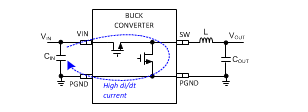
Radiated EMI is generated by the high di/dt components in pulsing currents in switching converters. The larger area covered by the path of a pulsing current, the more electromagnetic emission is generated. The key to minimize radiated EMI is to identify the pulsing current path and minimize the area of the path. In Buck converters,the pulsing current path is from the VIN side of the input capacitors to HS switch, to the LS switch, and then return to the ground of the input capacitors, as shown in Figure 106.
 Figure 106. Buck Converter High di / dt Path
High frequency ceramic bypass capacitors at the input side provide primary path for the high di/dt components of the pulsing current. Placing ceramic bypass capacitor(s) as close as possible to the VIN and PGND pins is the key to EMI reduction.
The SW pin connecting to the inductor should be as short as possible, and just wide enough to carry the load current without excessive heating. Short, thick traces or copper pours (shapes) should be used for high current condution path to minimize parasitic resistance. The output capacitors should be place close to the VOUT end of the inductor and closely grounded to PGND pin and exposed PAD.
The bypass capacitors on VCC and BIAS pins should be placed as close as possible to the pins respectively and closely grounded to PGND and the exposed PAD.