ZHCSCW6B August 2014 – January 2018 LM43601
PRODUCTION DATA.
- 1 特性
- 2 应用
- 3 说明
- 4 修订历史记录
- 5 Pin Configuration and Functions
- 6 Specifications
-
7 Detailed Description
- 7.1 Overview
- 7.2 Functional Block Diagram
- 7.3
Feature Description
- 7.3.1 Fixed-Frequency, Peak-Current-Mode Controlled, Step-Down Regulator
- 7.3.2 Light Load Operation
- 7.3.3 Adjustable Output Voltage
- 7.3.4 Enable (ENABLE)
- 7.3.5 VCC, UVLO and BIAS
- 7.3.6 Soft Start and Voltage Tracking (SS/TRK)
- 7.3.7 Switching Frequency (RT) and Synchronization (SYNC)
- 7.3.8 Minimum ON-Time, Minimum OFF-Time, and Frequency Foldback at Dropout Conditions
- 7.3.9 Internal Compensation and CFF
- 7.3.10 Bootstrap Voltage (BOOT)
- 7.3.11 Power Good (PGOOD)
- 7.3.12 Overcurrent and Short-Circuit Protection
- 7.3.13 Thermal Shutdown
- 7.4 Device Functional Modes
-
8 Applications and Implementation
- 8.1 Application Information
- 8.2
Typical Application
- 8.2.1 Design Requirements
- 8.2.2
Detailed Design Procedure
- 8.2.2.1 Custom Design With WEBENCH® Tools
- 8.2.2.2 Output Voltage Setpoint
- 8.2.2.3 Switching Frequency
- 8.2.2.4 Input Capacitors
- 8.2.2.5 Inductor Selection
- 8.2.2.6 Output Capacitor Selection
- 8.2.2.7 Feedforward Capacitor
- 8.2.2.8 Bootstrap Capacitors
- 8.2.2.9 VCC Capacitor
- 8.2.2.10 BIAS Capacitors
- 8.2.2.11 Soft-Start Capacitors
- 8.2.2.12 Undervoltage Lockout Set-Point
- 8.2.2.13 PGOOD
- 8.2.3 Application Curves
- 9 Power Supply Recommendations
- 10Layout
- 11器件和文档支持
- 12机械、封装和可订购信息
7.3.2 Light Load Operation
DCM operation is employed in the LM43601 when the inductor current valley reaches zero. The LM43601 is in DCM when load current is less than half of the peak-to-peak inductor current ripple in CCM. In DCM, the LS switch is turned off when the inductor current reaches zero. Switching loss is reduced by turning off the LS FET at zero current and the conduction loss is lowered by not allowing negative current conduction. Power conversion efficiency is higher in DCM than CCM under the same conditions.
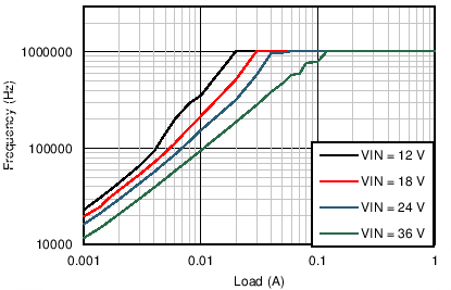
In DCM, the HS switch ON-time reduces with lower load current. When either the minimum HS switch ON-time (TON-MIN) or the minimum peak inductor current (IPEAK-MIN) is reached, the switching frequency decreases to maintain regulation. At this point, the LM43601 operates in PFM. In PFM, switching frequency is decreased by the control loop when load current reduces to maintain output voltage regulation. Switching loss is further reduced in PFM operation due to less frequent switching actions. Figure 34 shows an example of switching frequency decreases with decreased load current.
 Figure 34. Switching Frequency Decreases With Lower Load Current in PFM Operation
VOUT = 5 V, FS = 1 MHz
In PFM operation, a small, positive DC offset is required at the output voltage to activate the PFM detector. The lower the frequency in PFM, the more DC offset is needed at VOUT. See Typical Characteristics for typical DC offset at very light load. If the DC offset on VOUT is not acceptable for a given application, TI recommends a static load at output to reduce or eliminate the offset. Lowering values of the feedback divider RFBT and RFBB can also serve as a static load. In conditions with low VIN and/or high frequency, the LM43601 may not enter PFM mode if the output voltage cannot be charged up to provide the trigger to activate the PFM detector. Once the LM43601 is operating in PFM mode at higher VIN, the device remains in PFM operation when VIN is reduced.