ZHCSCC9C April 2014 – October 2017 LM43602
PRODUCTION DATA.
- 1 特性
- 2 应用
- 3 说明
- 4 修订历史记录
- 5 Pin Configuration and Functions
- 6 Specifications
-
7 Detailed Description
- 7.1 Overview
- 7.2 Functional Block Diagram
- 7.3
Feature Description
- 7.3.1 Fixed Frequency Peak Current-Mode Controlled Step-Down Regulator
- 7.3.2 Light Load Operation
- 7.3.3 Adjustable Output Voltage
- 7.3.4 Enable (EN)
- 7.3.5 VCC, UVLO and BIAS
- 7.3.6 Soft-Start and Voltage Tracking (SS/TRK)
- 7.3.7 Switching Frequency (RT) and Synchronization (SYNC)
- 7.3.8 Minimum ON-time, Minimum OFF-time and Frequency Foldback at Drop-Out Conditions
- 7.3.9 Internal Compensation and CFF
- 7.3.10 Bootstrap Voltage (BOOT)
- 7.3.11 Power Good (PGOOD)
- 7.3.12 Over Current and Short Circuit Protection
- 7.3.13 Thermal Shutdown
- 7.4 Device Functional Modes
-
8 Applications and Implementation
- 8.1 Application Information
- 8.2
Typical Applications
- 8.2.1 Design Requirements
- 8.2.2
Detailed Design Procedure
- 8.2.2.1 Custom Design With WEBENCH® Tools
- 8.2.2.2 Output Voltage Set-Point
- 8.2.2.3 Switching Frequency
- 8.2.2.4 Input Capacitors
- 8.2.2.5 Inductor Selection
- 8.2.2.6 Output Capacitor Selection
- 8.2.2.7 Feed-Forward Capacitor
- 8.2.2.8 Bootstrap Capacitors
- 8.2.2.9 VCC Capacitor
- 8.2.2.10 BIAS Capacitors
- 8.2.2.11 Soft-Start Capacitors
- 8.2.2.12 Under Voltage Lockout Set-Point
- 8.2.2.13 PGOOD
- 8.2.3 Application Performance Curves
- 9 Power Supply Recommendations
- 10Layout
- 11器件和文档支持
- 12机械、封装和可订购信息
封装选项
请参考 PDF 数据表获取器件具体的封装图。
机械数据 (封装 | 引脚)
- PWP|16
- DSU|16
散热焊盘机械数据 (封装 | 引脚)
- PWP|16
订购信息
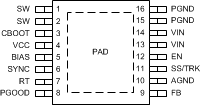
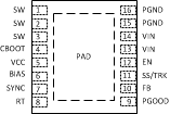
5 Pin Configuration and Functions
PWP Package
16-Pin HTSSOP
Top View

DSU Package
16-Pin VSON
Top View

Pin Functions
| PIN | DESCRIPTION | |||
|---|---|---|---|---|
| NAME | NUMBER | TYPE(1) | ||
| TSSOP | VSON | |||
| SW | 1,2 | 1,2,3 | P | Switching output of the regulator. Internally connected to both power MOSFETs. Connect to power inductor. |
| CBOOT | 3 | 4 | P | Boot-strap capacitor connection for high-side driver. Connect a high quality 470-nF capacitor from CBOOT to SW. |
| VCC | 4 | 5 | P | Internal bias supply output for bypassing. Connect bypass capacitor from this pin to AGND. Do not connect external loading to this pin. Never short this pin to ground during operation. |
| BIAS | 5 | 6 | P | Optional internal LDO supply input. To improve efficiency, it is recommended to tie to VOUT when 3.3 V ≤ VOUT ≤ 28 V, or tie to an external 3.3 V or 5 V rail if available. When used, place a bypass capacitor (1 to 10 µF) from this pin to ground. Tie to ground when not in use. |
| SYNC | 6 | 7 | A | Clock input to synchronize switching action to an external clock. Use proper high speed termination to prevent ringing. Connect to ground if not used. |
| RT | 7 | 8 | A | Connect a resistor RT from this pin to AGND to program switching frequency. Leave floating for 500 kHz default switching frequency. |
| PGOOD | 8 | 9 | A | Open drain output for power-good flag. Use a 10 kΩ to 100 kΩ pull-up resistor to logic rail or other DC voltage no higher than 12 V. |
| FB | 9 | 10 | A | Feedback sense input pin. Connect to the midpoint of feedback divider to set VOUT. Do not short this pin to ground during operation. |
| AGND | 10 | — | G | Analog ground pin. Ground reference for internal references and logic. Connect to system ground. |
| SS/TRK | 11 | 11 | A | Soft-start control pin. Leave floating for internal soft-start slew rate. Connect to a capacitor to extend soft start time. Connect to external voltage ramp for tracking. |
| EN | 12 | 12 | A | Enable input to the internal LDO and regulator. High = ON and low = OFF. Connect to VIN, or to VIN through resistor divider,or to an external voltage or logic source. Do not float. |
| VIN | 13,14 | 13,14 | P | Supply input pins to internal LDO and high side power FET. Connect to power supply and bypass capacitors CIN. Path from VIN pin to high frequency bypass CIN and PGND must be as short as possible. |
| PGND | 15,16 | 15,16 | G | Power ground pins, connected internally to the low side power FET. Connect to system ground, PAD, AGND, ground pins of CIN and COUT. Path to CIN must be as short as possible. |
| PAD | — | — | — | Low impedance connection to AGND. Connect to PGND on PCB. Major heat dissipation path of the die. Must be used for heat sinking to ground plane on PCB. |
(1) P = Power, A = Analog, G = Ground