ZHCSCN3B June 2014 – March 2018 LM46000
PRODUCTION DATA.
- 1 特性
- 2 应用
- 3 说明
- 4 修订历史记录
- 5 Pin Configuration and Functions
- 6 Specifications
-
7 Detailed Description
- 7.1 Overview
- 7.2 Functional Block Diagram
- 7.3
Feature Description
- 7.3.1 Fixed-Frequency, Peak-Current-Mode Controlled Step-Down Regulator
- 7.3.2 Light Load Operation
- 7.3.3 Adjustable Output Voltage
- 7.3.4 Enable (EN)
- 7.3.5 VCC, UVLO, and BIAS
- 7.3.6 Soft Start and Voltage Tracking (SS/TRK)
- 7.3.7 Switching Frequency (RT) and Synchronization (SYNC)
- 7.3.8 Minimum ON-Time, Minimum OFF-Time and Frequency Foldback at Dropout Conditions
- 7.3.9 Internal Compensation and CFF
- 7.3.10 Bootstrap Voltage (CBOOT)
- 7.3.11 Power Good (PGOOD)
- 7.3.12 Overcurrent and Short-Circuit Protection
- 7.3.13 Thermal Shutdown
- 7.4 Device Functional Modes
-
8 Applications and Implementation
- 8.1 Application Information
- 8.2
Typical Applications
- 8.2.1 Design Requirements
- 8.2.2
Detailed Design Procedure
- 8.2.2.1 Custom Design With WEBENCH® Tools
- 8.2.2.2 Output Voltage Setpoint
- 8.2.2.3 Switching Frequency
- 8.2.2.4 Input Capacitors
- 8.2.2.5 Inductor Selection
- 8.2.2.6 Output Capacitor Selection
- 8.2.2.7 Feed-Forward Capacitor
- 8.2.2.8 Bootstrap Capacitors
- 8.2.2.9 VCC Capacitor
- 8.2.2.10 BIAS Capacitors
- 8.2.2.11 Soft-Start Capacitors
- 8.2.2.12 Undervoltage Lockout Setpoint
- 8.2.2.13 PGOOD
- 8.2.3 Application Performance Curves
- 9 Power Supply Recommendations
- 10Layout
- 11器件和文档支持
- 12机械、封装和可订购信息
8.2 Typical Applications
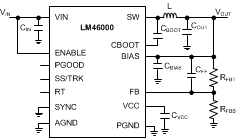
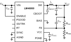
The LM46000 only requires a few external components to convert from a wide range of supply voltage to output voltage. Figure 44 shows a basic schematic when BIAS is connected to VOUT . This is recommended for VOUT ≥ 3.3 V. For VOUT< 3.3 V, connect BIAS to ground, as shown in Figure 45.
 Figure 44. LM46000 Basic Schematic for
VOUT ≥ 3.3 V, Tie BIAS to VOUT
 Figure 45. LM46000 Basic Schematic for
VOUT< 3.3 V, Tie BIAS to Ground
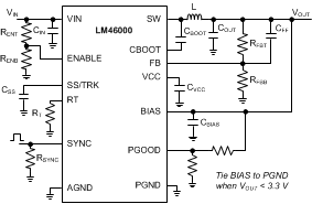
The LM46000 also integrates a full list of optional features to aid system design requirements, such as precision enable, VCC UVLO, programmable soft start, output voltage tracking, programmable switching frequency, clock synchronization and power-good indication. Each application can select the features for a more comprehensive design. A schematic with all features utilized is shown in Figure 46.

The external components must fulfill the needs of the application, but also the stability criteria of the device control loop. The LM46000 is optimized to work within a range of external components. Inductance and capacitance of the LC output filter must be considered in conjunction, creating a double pole, responsible for the corner frequency of the converter. Table 2 can be used to simplify the output filter component selection.
Table 2. L, COUT and CFF Typical Values
| FS (kHz) | L (µH)(1) | COUT (µF)(2) | CFF (pF)(3)(4) | RT (kΩ) | RFBB (kΩ)(3)(4) |
|---|---|---|---|---|---|
| VOUT = 1 V | |||||
| 200 | 22 | 500 | none | 200 | 100 |
| 500 | 10 | 330 | none | 80.6 or open | 100 |
| 1000 | 4.8 | 180 | none | 39.2 | 100 |
| 2200 | 2.2 | 100 | none | 17.8 | 100 |
| VOUT = 3.3 V | |||||
| 200 | 68 | 220 | 44 | 200 | 442 |
| 500 | 27 | 100 | 33 | 80.6 or open | 442 |
| 1000 | 15 | 47 | 18 | 39.2 | 442 |
| 2200 | 6.8 | 27 | 12 | 17.8 | 442 |
| VOUT = 5 V | |||||
| 200 | 100 | 150 | 66 | 200 | 249 |
| 500 | 44 | 66 | 33 | 80.6 or open | 249 |
| 1000 | 22 | 33 | 22 | 39.2 | 249 |
| 2200 | 10 | 22 | 18 | 17.8 | 249 |
| VOUT = 12 V | |||||
| 200 | 150 | 33 | see note (5) | 200 | 93.1 |
| 500 | 56 | 22 | 47 | 80.6 or open | 93.1 |
| 1000 | 27 | 15 | 33 | 39.2 | 93.1 |
| VOUT = 24 V | |||||
| 200 | 270 | 22 | see note (5) | 200 | 44.2 |
| 500 | 120 | 15 | see note (5) | 80.6 or open | 44.2 |
| 1000 | 56 | 10 | see note (5) | 39.2 | 44.2 |