ZHCSCD8C April 2014 – April 2019 LM46002
PRODUCTION DATA.
- 1 特性
- 2 应用
- 3 说明
- 4 修订历史记录
- 5 Pin Configuration and Functions
- 6 Specifications
-
7 Detailed Description
- 7.1 Overview
- 7.2 Functional Block Diagram
- 7.3
Feature Description
- 7.3.1 Fixed-Frequency, Peak-Current-Mode-Controlled, Step-Down Regulator
- 7.3.2 Light Load Operation
- 7.3.3 Adjustable Output Voltage
- 7.3.4 Enable (ENABLE)
- 7.3.5 VCC, UVLO, and BIAS
- 7.3.6 Soft Start and Voltage Tracking (SS/TRK)
- 7.3.7 Switching Frequency (RT) and Synchronization (SYNC)
- 7.3.8 Minimum ON-Time, Minimum OFF-Time, and Frequency Foldback at Dropout Conditions
- 7.3.9 Internal Compensation and CFF
- 7.3.10 Bootstrap Voltage (BOOT)
- 7.3.11 Power Good (PGOOD)
- 7.3.12 Overcurrent and Short-Circuit Protection
- 7.3.13 Thermal Shutdown
- 7.4 Device Functional Modes
-
8 Applications and Implementation
- 8.1 Application Information
- 8.2
Typical Applications
- 8.2.1 Design Requirements
- 8.2.2
Detailed Design Procedure
- 8.2.2.1 Custom Design With WEBENCH® Tools
- 8.2.2.2 Output Voltage Setpoint
- 8.2.2.3 Switching Frequency
- 8.2.2.4 Input Capacitors
- 8.2.2.5 Inductor Selection
- 8.2.2.6 Output Capacitor Selection
- 8.2.2.7 Feed-Forward Capacitor
- 8.2.2.8 Bootstrap Capacitors
- 8.2.2.9 VCC Capacitor
- 8.2.2.10 BIAS Capacitors
- 8.2.2.11 Soft-Start Capacitors
- 8.2.2.12 Undervoltage Lockout Setpoint
- 8.2.2.13 PGOOD
- 8.2.3 Application Performance Curves
- 9 Power Supply Recommendations
- 10Layout
- 11器件和文档支持
- 12机械、封装和可订购信息
10.1.2 Ground Plane and Thermal Considerations
TI recommends using one of the middle layers as a solid ground plane. Ground plane provides shielding for sensitive circuits and traces. It also provides a quiet reference potential for the control circuitry. The AGND and PGND pins should be connected to the ground plane using vias right next to the bypass capacitors. PGND pins are connected to the source of the internal LS switch. They should be connected directly to the grounds of the input and output capacitors. The PGND net contains noise at the switching frequency and may bounce due to load variations. The PGND trace, as well as PVIN and SW traces, should be constrained to one side of the ground plane. The other side of the ground plane contains much less noise and should be used for sensitive routes.
It is recommended to provide adequate device heat sinking by utilizing the PAD of the IC as the primary thermal path. Use a minimum 4 by 4 array of 10 mil thermal vias to connect the PAD to the system ground plane for heat sinking. The vias should be evenly distributed under the PAD. Use as much copper as possible for system ground plane on the top and bottom layers for the best heat dissipation. It is recommended to use a four-layer board with the copper thickness, for the four layers, starting from the top one, 2 oz / 1 oz / 1 oz / 2 oz. Four layer boards with enough copper thickness and proper layout provides low current conduction impedance, proper shielding and lower thermal resistance.
The thermal characteristics of the LM46002 are specified using the parameter RθJA, which characterize the junction temperature of the silicon to the ambient temperature in a specific system. Although the value of RθJA is dependant on many variables, it still can be used to approximate the operating junction temperature of the device. To obtain an estimate of the device junction temperature, one may use the following relationship:
where
- TJ = junction temperature in °C
- PD = VIN x IIN x (1 − Efficiency) − 1.1 × IOUT x DCR
- DCR = inductor DC parasitic resistance in Ω
- RθJA = junction-to-ambient thermal resistance of the device in °C/W
- TA = ambient temperature in °C.
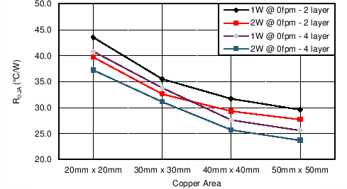
The maximum operating junction temperature of the LM46002 is 125°C. RθJA is highly related to PCB size and layout, as well as enviromental factors such as heat sinking and air flow. Figure 101 shows measured results of RθJA with different copper area on a 2-layer board and a 4-layer board.
 Figure 101. Measured RθJA vs PCB Copper Area on a 2-layer Board and a 4-layer Board