SNIS118G July 1999 – January 2017 LM50 , LM50-Q1
PRODUCTION DATA.
- 1 Features
- 2 Applications
- 3 Description
- 4 Revision History
- 5 Pin Configuration and Functions
- 6 Specifications
- 7 Detailed Description
- 8 Application and Implementation
- 9 Power Supply Recommendations
- 10Layout
- 11Device and Documentation Support
- 12Mechanical, Packaging, and Orderable Information
请参考 PDF 数据表获取器件具体的封装图。
机械数据 (封装 | 引脚)
- DBZ|3
散热焊盘机械数据 (封装 | 引脚)
7 Detailed Description
7.1 Overview
The LM50 and LM50-Q1 devices are precision integrated-circuit temperature sensors that can sense a –40°C to 125°C temperature range using a single positive supply. The output voltage of the LM50 and LM50-Q1 has a positive temperature slope of 10 mV/°C. A 500-mV offset is included enabling negative temperature sensing when biased by a single supply.
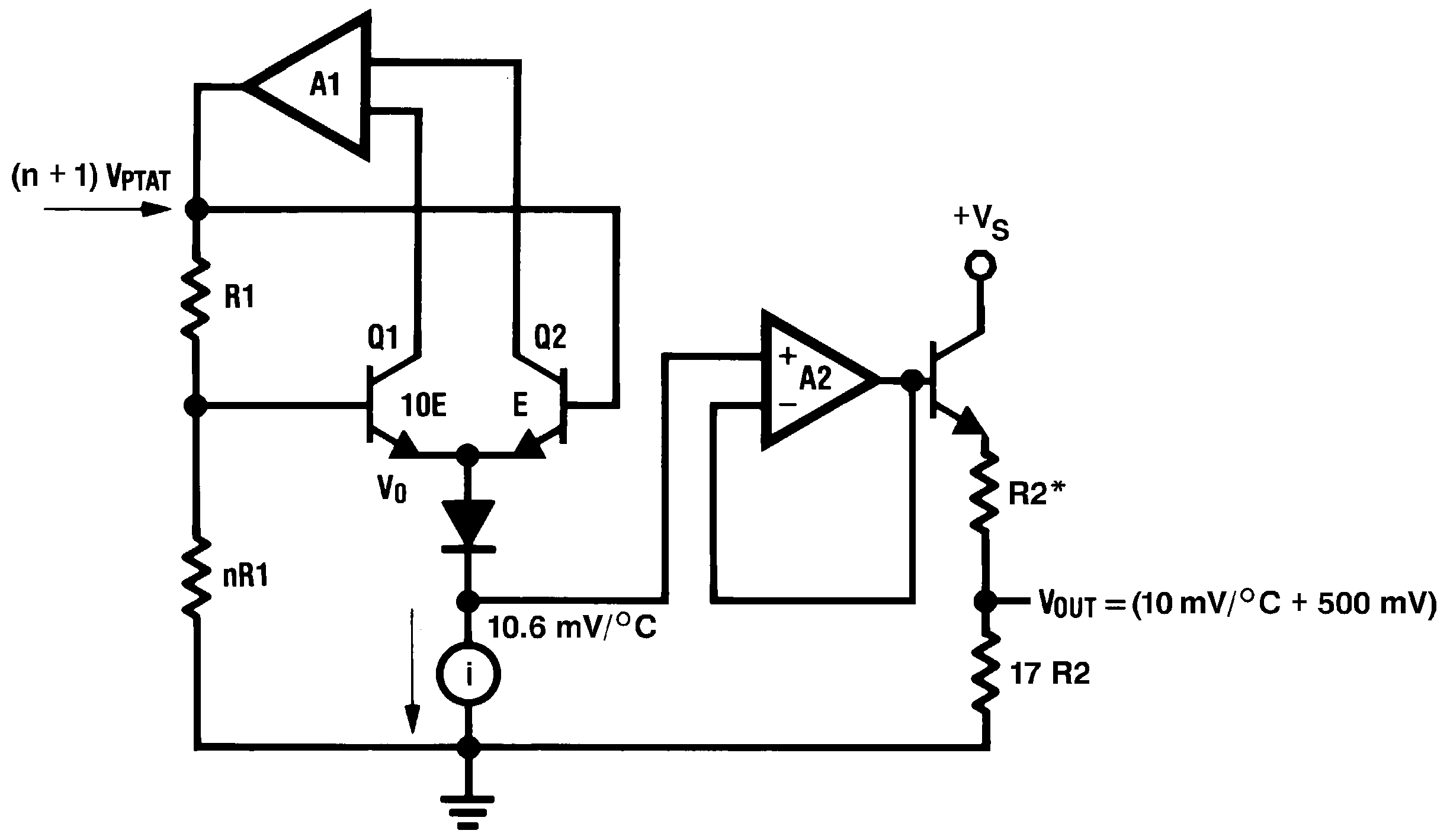
The temperature-sensing element is comprised of a delta-VBE architecture. The temperature-sensing element is then buffered by an amplifier and provided to the VOUT pin. The amplifier has a simple class A output stage with typical 2-kΩ output impedance as shown in the Functional Block Diagram.
7.2 Functional Block Diagram

7.3 Feature Description
7.3.1 LM50 and LM50-Q1 Transfer Function
The LM50 and LM50-Q1 follow a simple linear transfer function to achieve the accuracy as listed in the Electrical Characteristics: LM50B table and the Electrical Characteristics: LM50C and LM50-Q1 table.
Use Equation 1 to calculate the value of VO.
where
- T is the temperature in °C
- VO is the LM50 output voltage
7.4 Device Functional Modes
The only functional mode of the device has an analog output directly proportional to temperature.