SNVS484H January 2007 – July 2015 LM5001 , LM5001-Q1
PRODUCTION DATA.
- 1 Features
- 2 Applications
- 3 Description
- 4 Revision History
- 5 Pin Configuration and Functions
- 6 Specifications
- 7 Detailed Description
- 8 Applications and Implementation
- 9 Layout
- 10Device and Documentation Support
- 11Mechanical, Packaging, and Orderable Information
8 Applications and Implementation
NOTE
Information in the following applications sections is not part of the TI component specification, and TI does not warrant its accuracy or completeness. TI’s customers are responsible for determining suitability of components for their purposes. Customers should validate and test their design implementation to confirm system functionality.
8.1 Application Information
This information is intended to provide guidelines for the power supply designer using the LM5001.
8.1.1 VIN
The voltage applied to the VIN pin can vary within the range of 3.1 V to 75 V. The current into the VIN pin depends primarily on the gate charge of the power MOSFET, the switching frequency, and any external load on the VCC pin. It is recommended the filter shown in Figure 14 be used to suppress transients which may occur at the input supply. This is particularly important when VIN is operated close to the maximum operating rating of the LM5001.
When power is applied and the VIN voltage exceeds 2.8 V with the EN pin voltage greater than 0.45 V, the VCC regulator is enabled, supplying current into the external capacitor connected to the VCC pin. When the VIN voltage is between 2.8 V and 6.9 V, the VCC voltage is approximately equal to the VIN voltage. When the voltage on the VCC pin exceeds 6.9 V, the VCC pin voltage is regulated at 6.9 V. In typical flyback applications, an auxiliary transformer winding is connected through a diode to the VCC pin. This winding must raise the VCC voltage above 6.9 V to shut off the internal start-up regulator. The current requirements from this winding are relatively small, typically less than 20 mA. If the VIN voltage is much higher than the auxiliary voltage, the auxiliary winding significantly improves conversion efficiency. It also reduces the power dissipation within the LM5001. The externally applied VCC voltage should never exceed 14 V. Also the applied VCC should never exceed the VIN voltage to avoid reverse current through the internal VCC to VIN diode shown in the LM5001 block diagram.
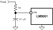 Figure 14. Input Transient Protection
8.1.2 SW Pin
Attention must be given to the PC board layout for the SW pin which connects to the power MOSFET drain. Energy can be stored in parasitic inductance and capacitance which cause switching spikes that negatively effect efficiency, and conducted and radiated emissions. These connections should be as short as possible to reduce inductance and as wide as possible to reduce resistance. The loop area, defined by the SW and GND pin connections, the transformer or inductor terminals, and their respective return paths, should be minimized.
8.1.3 EN / UVLO Voltage Divider Selection
Two dedicated comparators connected to the EN pin are used to detect under-voltage and shutdown conditions. When the EN pin voltage is below 0.45 V, the controller is in a low current shutdown mode where the VIN current is reduced to 95 µA. For an EN pin voltage greater than 0.45 V but less than 1.26 V the controller is in standby mode, with all internal circuits operational, but the PWM gate driver signal is blocked. Once the EN pin voltage is greater than 1.26 V, the controller is fully enabled. Two external resistors can be used to program the minimum operational voltage for the power converter as shown in Figure 15. When the EN pin voltage falls below the 1.26 V threshold, an internal 100 mV threshold hysteresis prevents noise from toggling the state, so the voltage must be reduced to 1.16 V to transition to standby. Resistance values for R1 and R2 can be determined from Equation 2 and Equation 3:


where VPWR is the desired turn-on voltage and IDIVIDER is an arbitrary current through R1 and R2.
For example, if the LM5001 is to be enabled when VPWR reaches 16 V, IDIVIDER could be chosen as 501 µA which would set R1 to 29.4 kΩ and R2 to 2.49 kΩ. The voltage at the EN pin should not exceed 10 V unless the current into the 6 V protection Zener diode is limited below 4 mA. The EN pin voltage should not exceed 14 V at any time. Be sure to check both the power and voltage rating (some 0603 resistors are rated as low as 50 V) for the selected R1 resistor.
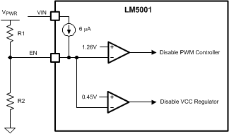 Figure 15. Basic EN (UVLO) Configuration
Remote configuration of the controller’s operational modes can be accomplished with open drain device(s) connected to the EN pin as shown in Figure 16. A MOSFET or an NPN transistor connected to the EN pin can force the regulator into the low power ‘off’ state. Adding a PN diode in the drain (or collector) provides the offset to achieve the standby state. The advantage of standby is that the VCC LDO is not disabled and external circuitry powered by VCC remains functional.
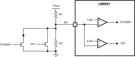 Figure 16. Remote Standby and Disable Control
8.1.4 Soft-Start
Soft-start (SS) can be implemented with an external capacitor connected to COMP through a diode as shown in Figure 17. The COMP discharge MOSFET conducts during Shutdown and Standby modes to keep the COMP voltage below the PWM offset (1.3 V), which inhibits PWM pulses. The error amplifier attempts to raise the COMP voltage after the EN pin exceeds the 1.26-V standby threshold. Because the error amplifier output can only sink current, the internal COMP pull-up resistor (~5 kΩ) supplies the charging current to the SS capacitor. The SS capacitor causes the COMP voltage to gradually increase, until the output voltage achieves regulation and FB assumes control of the COMP and the PWM duty cycle. The SS capacitor continues charging through a large resistance, RSS, preventing the SS circuit from interfering with the normal error amplifier function. During shutdown, the VCC diode discharges the SS capacitor.
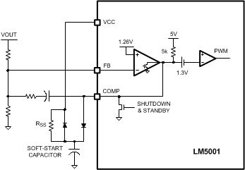 Figure 17. Soft-Start
8.2 Typical Applications
Figure 18, Figure 19, Figure 20, Figure 21, and Figure 22 present examples of a Non-Isolated Flyback, Isolated Flyback, Boost, 24-V SEPIC and a 12-V Automotive range SEPIC converters utilizing the LM5001 switching regulator.
8.2.1 Non-Isolated Flyback
The Non-Isolated Flyback converter (Figure 18) utilizes the internal voltage reference for the regulation setpoint. The output is 5 V at 1 A while the input voltage can vary from 16 V to 42 V. The switching frequency is set to 250 kHz. An auxiliary winding on transformer (T1) provides 7.5 V to power the LM5001 when the output is in regulation. This disables the internal high voltage VCC LDO regulator and improves efficiency. The input under-voltage threshold is 13.9 V. The converter can be shut down by driving the EN input below 1.26 V with an open-collector or open-drain transistor. An external synchronizing frequency can be applied to the SYNC input. An optional soft-start circuit is connected to the COMP pin input. When power is applied, the soft-start capacitor (C7) is discharged and limits the voltage applied to the PWM comparator by the internal error amplifier. The internal ~5 kΩ COMP pull-up resistor charges the soft-start capacitor until regulation is achieved. The VCC pull-up resistor (R7) continues to charge C7 so that the soft-start circuit will not affect the compensation network in normal operation. If the output capacitance is small, the soft-start circuit can be adjusted to limit the power-on output voltage overshoot. If the output capacitance is sufficiently large, no soft-start circuit is needed because the LM5001 gradually charges the output capacitor by current limiting at approximately 1 A (ILIM) until regulation is achieved.
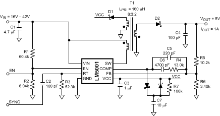 Figure 18. Non-Isolated Flyback
8.2.2 Isolated Flyback
The Isolated Flyback converter (Figure 19) utilizes a 2.5 V voltage reference (LM431) located on the isolated secondary side for the regulation setpoint. The LM5001 internal error amplifier is disabled by grounding the FB pin. The LM431 controls the current through the opto-coupler LED, which sets the COMP pin voltage. The R4 and C3 network boosts the phase response of the opto-coupler to increase the loop bandwidth. The output is 5 V at 1 A and the input voltage ranges from 16 V to 42 V. The switching frequency is set to 250 kHz.
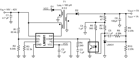 Figure 19. Isolated Flyback
8.2.3 Boost
The Boost converter (Figure 20) utilizes the internal voltage reference for the regulation setpoint. The output is 48 V at 150 mA, while the input voltage can vary from 16 V to 36 V. The switching frequency is set to 250 kHz. The internal VCC regulator provides 6.9 V bias power, since there isn’t a simple method for creating an auxiliary voltage with the boost topology. Note that the boost topology does not provide output short-circuit protection because the power MOSFET cannot interrupt the path between the input and the output.
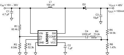 Figure 20. Boost
8.2.4 24-V SEPIC
The 24-V SEPIC converter (Figure 21) utilizes the internal voltage reference for the regulation setpoint. The output is 24 V at 250 mA while the input voltage can vary from 16 V to 48 V. The switching frequency is set to 250 kHz. The internal VCC regulator provides 6.9 V bias power for the LM5001. An auxiliary voltage can be created by adding a winding on L2 and a diode into the VCC pin.
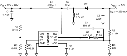 Figure 21. 24-V SEPIC
8.2.5 12-V Automotive SEPIC
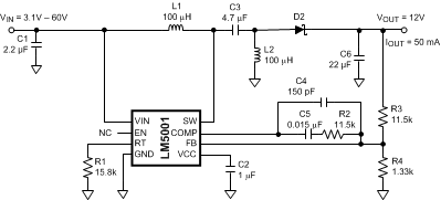
The 12-V Automotive SEPIC converter (Figure 22) utilizes the internal bandgap voltage reference for the regulation setpoint. The output is 12 V at 50 mA while the input voltage can vary from 3.1 V to 60 V. The output current rating can be increased if the minimum VIN voltage requirement is increased. The switching frequency is set to 750 kHz. The internal VCC regulator provides 6.9 V bias power for the LM5001. The output voltage can be used as an auxiliary voltage if the nominal VIN voltage is greater than 12 V by adding a diode from the output into the VCC pin. In this configuration, the minimum input voltage must be greater than 12 V to prevent the internal VCC to VIN diode from conducting. If the applied VCC voltage exceeds the minimum VIN voltage, then an external blocking diode is required between the VIN pin and the power source to block current flow from VCC to the input supply.
