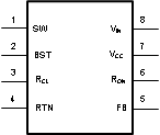
| 1 |
SW |
O |
Switching node. |
Power switching node. Connect to the LC output filter. |
| 2 |
BST |
I |
Boost bootstrap capacitor input. |
An external capacitor is required between the BST and SW pins. A 0.01-µF ceramic capacitor is recommended. An internal diode between VCC and BST completes the buck gate drive bias network. |
| 3 |
RCL |
I |
Current Limit OFF-time programming pin
tOFF = 10-5 / (0.59 + (VFB / 7.22 × 10− 6 × RCL)) |
A resistor between this pin and RTN determines the variation of off-time along with the FB pin voltage per cycle while in current limit. The off-time is preset to 17 µs if FB = 0 V and decreases as the FB voltage increases. |
| 4 |
RTN |
— |
Circuit ground. |
|
| 5 |
FB |
I |
Feedback signal from regulated output. |
This pin is connected to the inverting input of the internal regulation comparator. The regulation threshold is 2.5 V. |
| 6 |
RON |
I |
On-time set pin
tON = 1.42 × 10⁻¹⁰ RON / VIN |
A resistor between this pin and VIN sets the switch on-time as a function of VIN. The minimum recommended on-time is 300 ns at the maximum input voltage. |
| 7 |
VCC |
O |
Output from the internal high-voltage bias regulator. VCC is nominally regulated to 7 V. |
If an auxiliary voltage is available to raise the voltage on this pin, above the regulation set point (7V), the internal series pass regulator will shutdown, reducing the IC power dissipation. Do not exceed 14V. This output provides gate drive power for the internal buck switch. An internal diode is provided between this pin and the BST pin. A local 0.1-uF decoupling capacitor is recommended. The series pass regulator is current limited to 10 mA. |
| 8 |
VIN |
I |
Input supply voltage. |
Recommended operating range: 9 V to 75 V. |
| — |
EP |
— |
Exposed PAD, underside of the WSON-8 package option. |
Internally bonded to the die substrate. Connect to GND potential for low thermal impedance. |
