ZHCSIX0H March 2009 – October 2018 LM5008A
PRODUCTION DATA.
8.2.2.3 Low-Output Ripple Configurations
For applications where low-output ripple is required, the following options can be used to reduce or nearly eliminate the ripple:
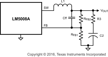
- Reduced ripple configuration: In Figure 11, Cff is added across RFB2 to AC-couple the ripple at VOUT directly to the FB pin. This allows the ripple at VOUT to be reduced to a minimum of 25 mVp-p by reducing R3, because the ripple at VOUT is not attenuated by the feedback resistors. The minimum value for Cff is determined by Equation 10:
- tON(max) is the maximum on-time, which occurs at VIN(min). The next larger standard value capacitor must be used for Cff.
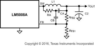
- Minimum ripple configuration: If the application requires a lower value of ripple (<10 mVp-p), the circuit of Figure 12 can be used. R3 is removed, and the resulting output ripple voltage is determined by the inductor’s ripple current and C2’s characteristics. RA and CA are chosen to generate a sawtooth waveform at their junction, and that voltage is AC-coupled to the FB pin through CB. To determine the values for RA, CA, and CB, use the following procedure in Equation 11:
- VSW is the absolute value of the voltage at the SW pin during the off-time (typically 1 V). VA is the DC voltage at the RA/CA junction, and is used in Equation 12.
- tON is the maximum on-time (at minimum input voltage), and ΔV is the desired ripple amplitude at the RA/CA junction (typically 40-50 mV). RA and CA are then chosen from standard value components to satisfy the above product. Typically CA is 1000 pF to 5000 pF, and RA is 10 kΩ to 300 kΩ. CB is then chosen large compared to CA, typically 0.1 µF.
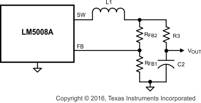
- Alternate minimum ripple configuration: The circuit in Figure 13 is the same as that in the Functional Block Diagram, except the output voltage is taken from the junction of R3 and C2. The ripple at VOUT is determined by the inductor’s ripple current and C2’s characteristics. However, R3 slightly degrades the load regulation. This circuit may be suitable if the load current is fairly constant.
Equation 10. 

where
 Figure 11. Reduced Ripple Configuration
 Equation 11. Calculate VA = VOUT – (VSW × (1 – (VOUT/VIN(min))))
where
Equation 12. Calculate RA × CA = (VIN(min) – VA) × tON/ΔV
where
 Figure 12. Minimum Output Ripple Using Ripple Injection