SNVS376F October 2005 – May 2016 LM5010A , LM5010A-Q1
PRODUCTION DATA.
- 1 Features
- 2 Applications
- 3 Description
- 4 Revision History
- 5 Pin Configuration and Functions
- 6 Specifications
- 7 Detailed Description
- 8 Application and Implementation
- 9 Power Supply Recommendations
- 10Layout
- 11Device and Documentation Support
- 12Mechanical, Packaging, and Orderable Information
封装选项
机械数据 (封装 | 引脚)
散热焊盘机械数据 (封装 | 引脚)
- PWP|14
订购信息
10 Layout
10.1 Layout Guidelines
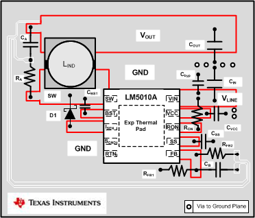
The LM5010Ax regulation, overvoltage, and current limit comparators are very fast, and respond to short duration noise pulses. Therefore, layout considerations are critical for optimum performance. The layout must be as neat and compact as possible, and all the components must be as close as possible to their associated pins. The two major current loops have currents which switch very fast, and so the loops should be as small as possible to minimize conducted and radiated EMI. The first loop is that formed by C1 (CIN), through the VIN to SW pins, L1 (LIND), C2 (COUT), and back to C1. The second loop is that formed by D1, L1, C2, and the SGND and ISEN pins. The ground connection from C2 to C1 should be as short and direct as possible, preferably without going through vias. Directly connect the SGND and RTN pin to each other, and they should be connected as directly as possible to the C1/C2 ground line without going through vias. The power dissipation within the IC can be approximated by determining the total conversion loss (PIN - POUT), and then subtracting the power losses in the free-wheeling diode and the inductor. The power loss in the diode is approximately Equation 27.
where
- IO is the load current
- VF is the diode’s forward voltage drop
- D is the duty cycle
The power loss in the inductor is approximately Equation 28.
where
- RL is the inductor’s DC resistance
- the 1.1 factor is an approximation for the AC losses
If it is expected that the internal dissipation of the LM5010Ax will produce high junction temperatures during normal operation, good use of the PC board’s ground plane can help considerably to dissipate heat. The exposed pad on the IC package bottom should be soldered to a ground plane, and that plane should both extend from beneath the IC, and be connected to exposed ground plane on the board’s other side using as many vias as possible. The exposed pad is internally connected to the IC substrate. The use of wide PC board traces at the pins, where possible, can help conduct heat away from the IC. The four no connect pins on the HTSSOP package are not electrically connected to any part of the IC, and may be connected to ground plane to help dissipate heat from the package. Judicious positioning of the PC board within the end product, along with the use of any available air flow (forced or natural convection) can help reduce the junction temperature.
10.2 Layout Example
 Figure 18. LM5010A Buck Layout Example With the WSON Package