ZHCSES8 March 2016 LM5022-Q1
PRODUCTION DATA.
- 1 特性
- 2 应用
- 3 说明
- 4 修订历史记录
- 5 Pin Configuration and Functions
- 6 Specifications
- 7 Detailed Description
-
8 Application and Implementation
- 8.1 Application Information
- 8.2
Typical Application
- 8.2.1 Design Requirements
- 8.2.2
Detailed Design Procedure
- 8.2.2.1 Switching Frequency
- 8.2.2.2 MOSFET
- 8.2.2.3 Output Diode
- 8.2.2.4 Boost Inductor
- 8.2.2.5 Output Capacitor
- 8.2.2.6 VCC Decoupling Capacitor
- 8.2.2.7 Input Capacitor
- 8.2.2.8 Current Sense Filter
- 8.2.2.9 RSNS, RS2 and Current Limit
- 8.2.2.10 Control Loop Compensation
- 8.2.2.11 Efficiency Calculations
- 8.2.3 Application Curves
- 9 Power Supply Recommendations
- 10Layout
- 11器件和文档支持
- 12机械、封装和可订购信息
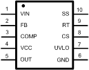
5 Pin Configuration and Functions
DGS Package
10-Pin VSSOP
Top View

Pin Functions
| PIN | TYPE | DESCRIPTION | APPLICATION INFORMATION | |
|---|---|---|---|---|
| NO. | NAME | |||
| 1 | VIN | I | Source input voltage | Input to the start-up regulator. Operates from 6 V to 60 V. |
| 2 | FB | I | Feedback pin | Inverting input to the internal voltage error amplifier. The non-inverting input of the error amplifier connects to a 1.25-V reference. |
| 3 | COMP | I/O | Error amplifier output and PWM comparator input | The control loop compensation components connect between this pin and the FB pin. |
| 4 | VCC | O | Output of the internal, high voltage linear regulator. | This pin should be bypassed to the GND pin with a ceramic capacitor. |
| 5 | OUT | O | Output of MOSFET gate driver | Connect this pin to the gate of the external MOSFET. The gate driver has a 1-A peak current capability. |
| 6 | GND | - | System ground | |
| 7 | UVLO | I | Input undervoltage lockout | Set the start-up and shutdown levels by connecting this pin to the input voltage through a resistor divider. A 20-µA current source provides hysteresis. |
| 8 | CS | I | Current sense input | Input for the switch current used for current mode control and for current limiting. |
| 9 | RT/SYNC | I | Oscillator frequency adjust pin and synchronization input | An external resistor connected from this pin to GND sets the oscillator frequency. This pin can also accept an AC-coupled input for synchronization from an external clock. |
| 10 | SS | I | Soft-start pin | An external capacitor placed from this pin to ground will be charged by a 10-µA current source, creating a ramp voltage to control the regulator start-up. |