ZHCSES8 March 2016 LM5022-Q1
PRODUCTION DATA.
- 1 特性
- 2 应用
- 3 说明
- 4 修订历史记录
- 5 Pin Configuration and Functions
- 6 Specifications
- 7 Detailed Description
-
8 Application and Implementation
- 8.1 Application Information
- 8.2
Typical Application
- 8.2.1 Design Requirements
- 8.2.2
Detailed Design Procedure
- 8.2.2.1 Switching Frequency
- 8.2.2.2 MOSFET
- 8.2.2.3 Output Diode
- 8.2.2.4 Boost Inductor
- 8.2.2.5 Output Capacitor
- 8.2.2.6 VCC Decoupling Capacitor
- 8.2.2.7 Input Capacitor
- 8.2.2.8 Current Sense Filter
- 8.2.2.9 RSNS, RS2 and Current Limit
- 8.2.2.10 Control Loop Compensation
- 8.2.2.11 Efficiency Calculations
- 8.2.3 Application Curves
- 9 Power Supply Recommendations
- 10Layout
- 11器件和文档支持
- 12机械、封装和可订购信息
6 Specifications
6.1 Absolute Maximum Ratings
over operating free-air temperature range (unless otherwise noted)(1)(2)| MIN | MAX | UNIT | ||
|---|---|---|---|---|
| VIN to GND | –0.3 | 65 | V | |
| VCC to GND | –0.3 | 16 | V | |
| RT/SYNC to GND | –0.3 | 5.5 | V | |
| OUT to GND | –1.5V for < 100 ns | |||
| All other pins to GND | –0.3 | 7 | V | |
| Power dissipation | Internally limited | |||
| Junction temperature(3) | 150 | °C | ||
| Soldering information | Vapor phase (60 sec.) | 215 | °C | |
| Infrared (15 sec.) | 220 | °C | ||
| Storage temperature, Tstg | –65 | 150 | °C | |
(1) Stresses beyond those listed under Absolute Maximum Ratings may cause permanent damage to the device. These are stress ratings only, which do not imply functional operation of the device at these or any other conditions beyond those indicated under Recommended Operating Conditions. Exposure to absolute-maximum-rated conditions for extended periods may affect device reliability.
(2) If Military/Aerospace specified devices are required, contact the Texas Instruments Sales Office/ Distributors for availability and specifications.
(3) High junction temperatures degrade operating lifetimes. Operating lifetime is de-rated for junction temperatures greater than 125°C.
6.2 ESD Ratings: LM5022-Q1
| VALUE | UNIT | |||
|---|---|---|---|---|
| V(ESD) | Human body model (HBM), per AEC Q100-002(1) | ±2000 | V | |
| Charged device model (CDM), per AEC Q100-011(2) | ±750 | V | ||
(1) AEC Q100-002 indicates HBM stressing is done in accordance with the ANSI/ESDA/JEDEC JS-001 specification. This is the passing level per ANSI/ESDA/JEDEC JS-001. JEDEC document JEP155 states that 500 V HBM allows safe manufacturing with a standard ESD control process
(2) Level listed above is the passing level per EIA-JEDEC JESD22-C101. JEDEC document JEP157 states that 250 V CDM allows safe manufacturing with a standard ESD control process.
6.3 Recommended Operating Conditions
over operating free-air temperature range (unless otherwise noted)(1)| MIN | NOM | MAX | UNIT | ||
|---|---|---|---|---|---|
| Supply voltage | 6 | 60 | V | ||
| External voltage at VCC | 7.5 | 14 | V | ||
| Junction temperature | –40 | 125 | °C | ||
(1) Operating Ratings are conditions under the device is intended to be functional. For specifications and test conditions, see Electrical Characteristics
6.4 Thermal Information
| THERMAL METRIC(1) | LM5022-Q1 | UNIT | |
|---|---|---|---|
| DGS (VSSOP) | |||
| 10 PINS | |||
| RθJA | Junction-to-ambient thermal resistance | 161.5 | °C/W |
| RθJC(top) | Junction-to-case (top) thermal resistance | 56 | °C/W |
| RθJB | Junction-to-board thermal resistance | 81.3 | °C/W |
| ψJT | Junction-to-top characterization parameter | 5.7 | °C/W |
| ψJB | Junction-to-board characterization parameter | 80 | °C/W |
| RθJC(bot) | Junction-to-case (bottom) thermal resistance | N/A | °C/W |
(1) For more information about traditional and new thermal metrics, see the Semiconductor and IC Package Thermal Metrics application report, SPRA953.
6.5 Electrical Characteristics
Typical limits apply for TJ = 25°C and are provided for reference purposes only; minimum and maximum limits apply over the junction temperature (TJ) range of –40°C to +125°C. VIN = 24 V and RT = 27.4 kΩ, unless otherwise indicated.(1)| PARAMETER | TEST CONDITIONS | MIN | TYP | MAX | UNIT | |
|---|---|---|---|---|---|---|
| SYSTEM PARAMETERS | ||||||
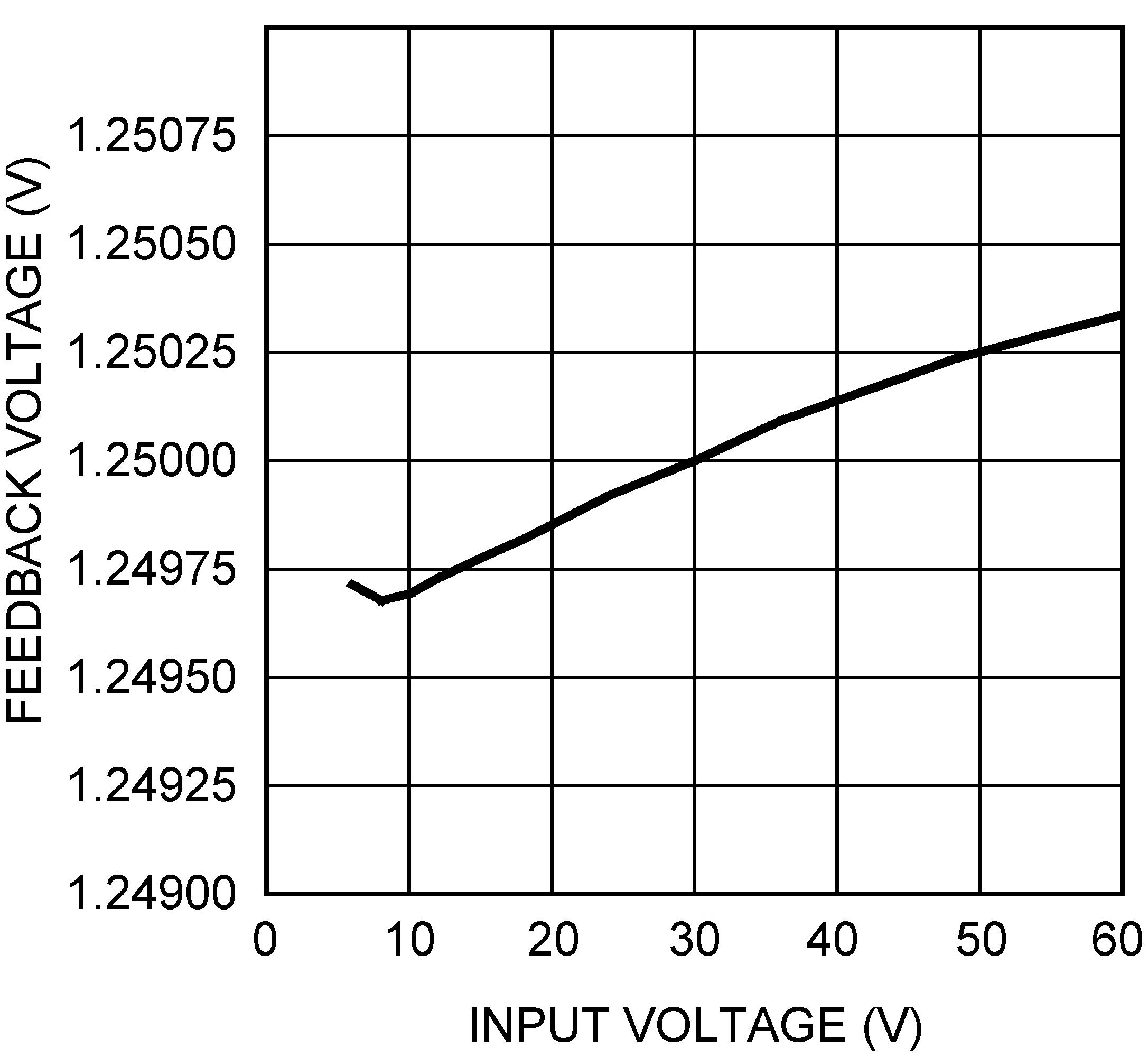
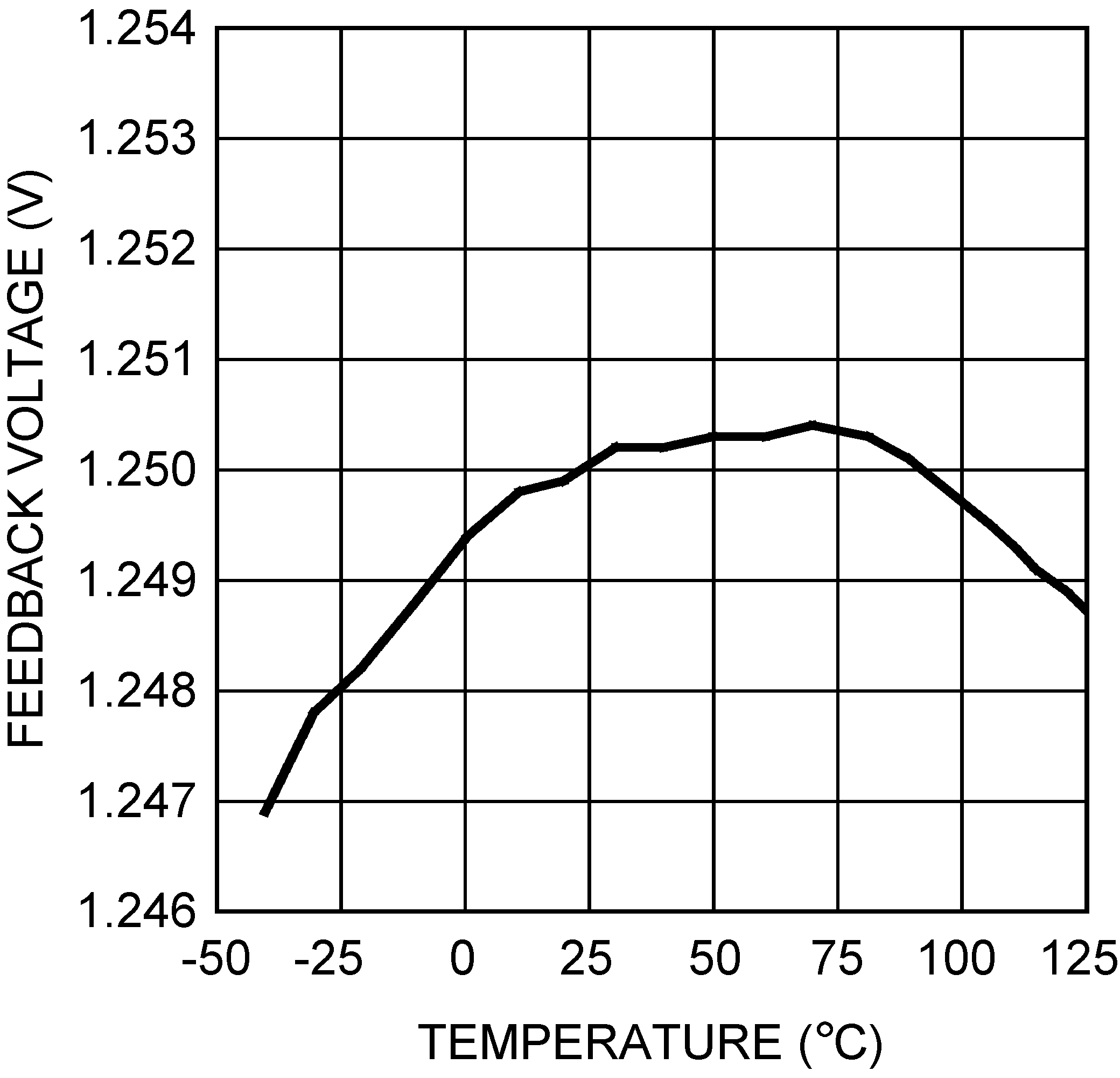
| VFB | FB Pin Voltage | 1.225 | 1.250 | 1.275 | V | |
| START-UP REGULATOR | ||||||
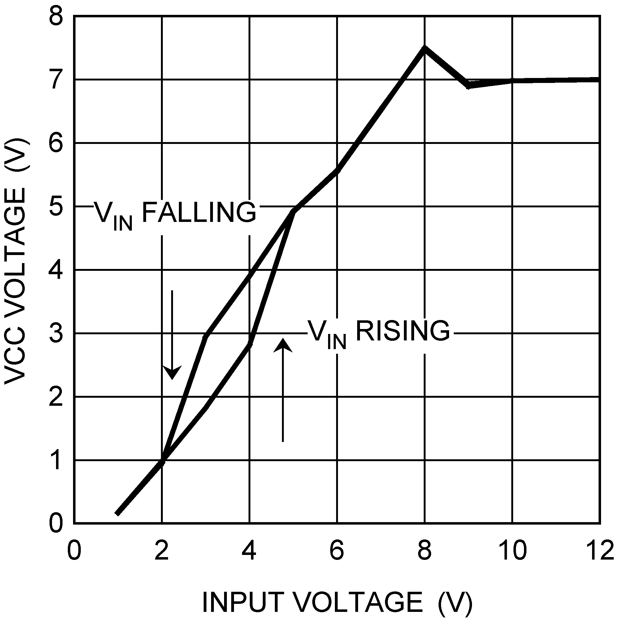
| VCC(2) | VCC Regulation | 10 V ≤ VIN ≤ 60 V, ICC = 1 mA | 6.6 | 7 | 7.4 | V |
| VCC Regulation | 6 V ≤ VIN < 10 V, VCC Pin Open Circuit | 5 | ||||
| ICC | Supply Current | OUT Pin Capacitance = 0 VCC = 10 V |
3.5 | 4 | mA | |
| ICC-LIM | VCC Current Limit | VCC = 0 V, ((3), (2)) | 15 | 35 | mA | |
| VIN - VCC | Dropout Voltage Across Bypass Switch | ICC = 0 mA, ƒSW < 200 kHz 6 V ≤ VIN ≤ 8.5 V |
200 | mV | ||
| VBYP-HI | Bypass Switch Turn-off Threshold | VIN increasing | 8.7 | V | ||
| VBYP-HYS | Bypass Switch Threshold Hysteresis | VIN Decreasing | 260 | mV | ||
| ZVCC | VCC Pin Output Impedance 0 mA ≤ ICC ≤ 5 mA |
VIN = 6 V | 58 | Ω | ||
| VIN = 8 V | 53 | |||||
| VIN = 24 V | 1.6 | |||||
| VCC-HI | VCC Pin UVLO Rising Threshold | 5 | V | |||
| VCC-HYS | VCC Pin UVLO Falling Hysteresis | 300 | mV | |||
| IVIN | Start-up Regulator Leakage | VIN = 60 V | 150 | 500 | µA | |
| IIN-SD | Shutdown Current | VUVLO = 0 V, VCC = Open Circuit | 350 | 450 | µA | |
| ERROR AMPLIFIER | ||||||
| GBW | Gain Bandwidth | 4 | MHz | |||
| ADC | DC Gain | 75 | dB | |||
| ICOMP | COMP Pin Current Sink Capability | VFB = 1.5 V VCOMP = 1 V |
5 | 17 | mA | |
| UVLO | ||||||
| VSD | Shutdown Threshold | 1.22 | 1.25 | 1.28 | V | |
| ISD-HYS | Shutdown Hysteresis Current Source |
16 | 20 | 24 | µA | |
| CURRENT LIMIT | ||||||
| tLIM-DLY | Delay from ILIM to Output | CS steps from 0 V to 0.6 V OUT transitions to 90% of VCC |
30 | ns | ||
| VCS | Current Limit Threshold Voltage | 0.434 | 0.5 | 0.55 | V | |
| tBLK | Leading Edge Blanking Time | 65 | ns | |||
| RCS | CS Pin Sink Impedance | Blanking active | 40 | 75 | Ω | |
| SOFT-START | ||||||
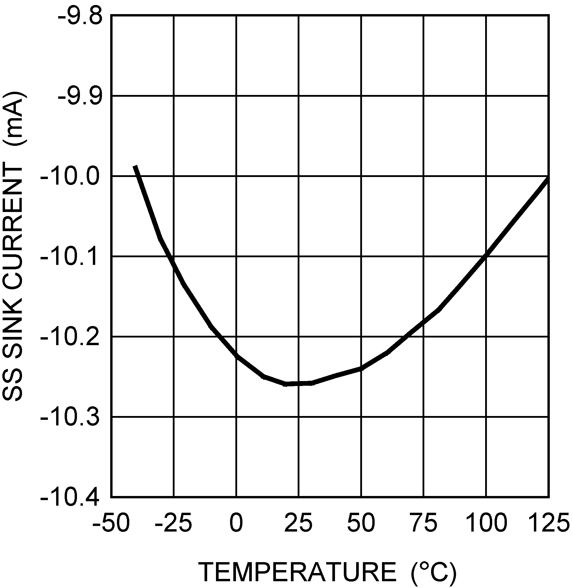
| ISS | Soft-start Current Source | 7 | 10 | 13 | µA | |
| VSS-OFF | Soft-start to COMP Offset | 0.344 | 0.55 | 0.75 | V | |
| OSCILLATOR | ||||||
| fSW | RT to GND = 84.5 kΩ | See(4) | 170 | 200 | 230 | kHz |
| RT to GND = 27.4 kΩ | See(4) | 525 | 600 | 675 | kHz | |
| RT to GND = 16.2 kΩ | See(4) | 865 | 990 | 1115 | kHz | |
| RT to GND = 6.65 kΩ | See(4) | 1910 | 2240 | 2570 | kHz | |
| VSYNC-HI | Synchronization Rising Threshold | 3.8 | V | |||
| PWM COMPARATOR | ||||||
| tCOMP-DLY | Delay from COMP to OUT Transition | VCOMP = 2 V CS stepped from 0 V to 0.4 V |
25 | ns | ||
| DMIN | Minimum Duty Cycle | VCOMP = 0 V | 0% | |||
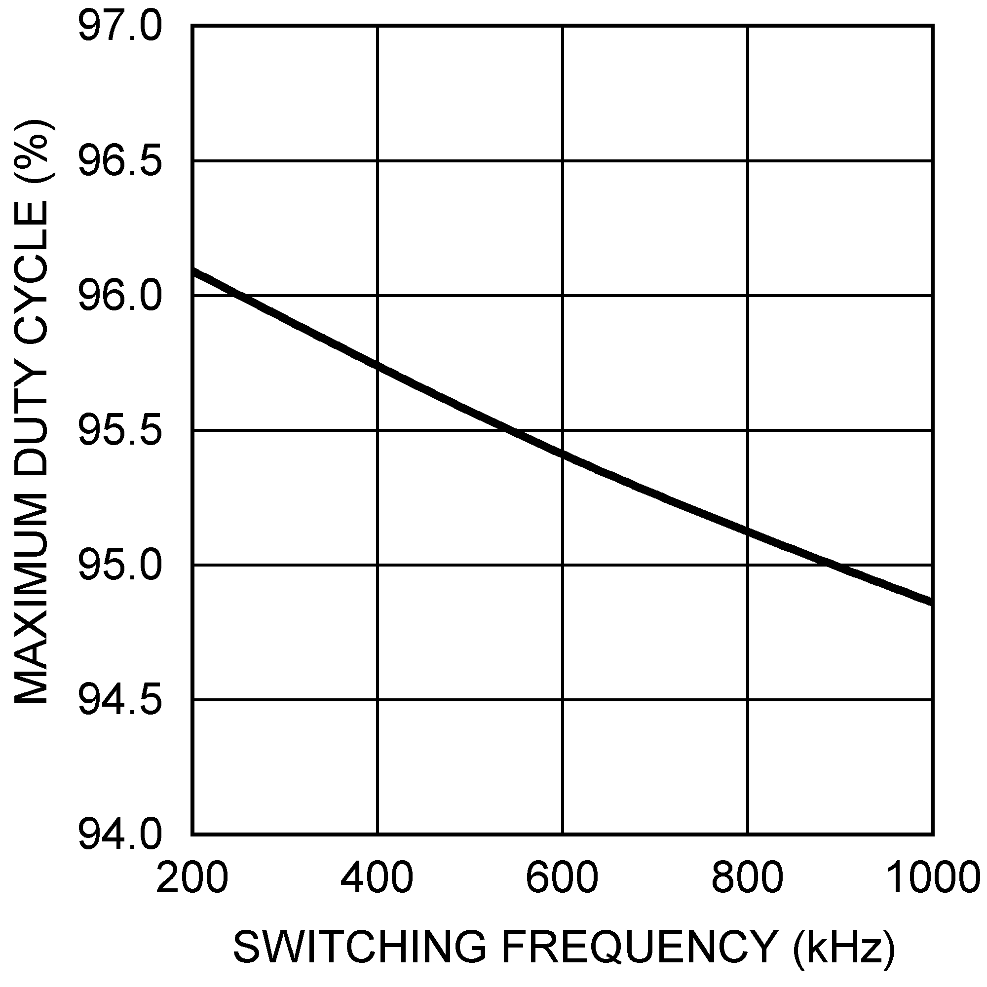
| DMAX | Maximum Duty Cycle | 90% | 95% | |||
| APWM | COMP to PWM Comparator Gain | 0.33 | V/V | |||
| VCOMP-OC | COMP Pin Open Circuit Voltage | VFB = 0 V | 4.3 | 5.2 | 6.1 | V |
| ICOMP-SC | COMP Pin Short Circuit Current | VCOMP = 0 V, VFB = 0V | 0.6 | 1.1 | 1.5 | mA |
| SLOPE COMPENSATION | ||||||
| VSLOPE | Slope Compensation Amplitude | 83 | 110 | 137 | mV | |
| MOSFET DRIVER | ||||||
| VSAT-HI | Output High Saturation Voltage (VCC – VOUT) | IOUT = 50 mA | 0.25 | 0.75 | V | |
| VSAT-LO | Output Low Saturation Voltage (VOUT) | IOUT = 100 mA | 0.25 | 0.75 | V | |
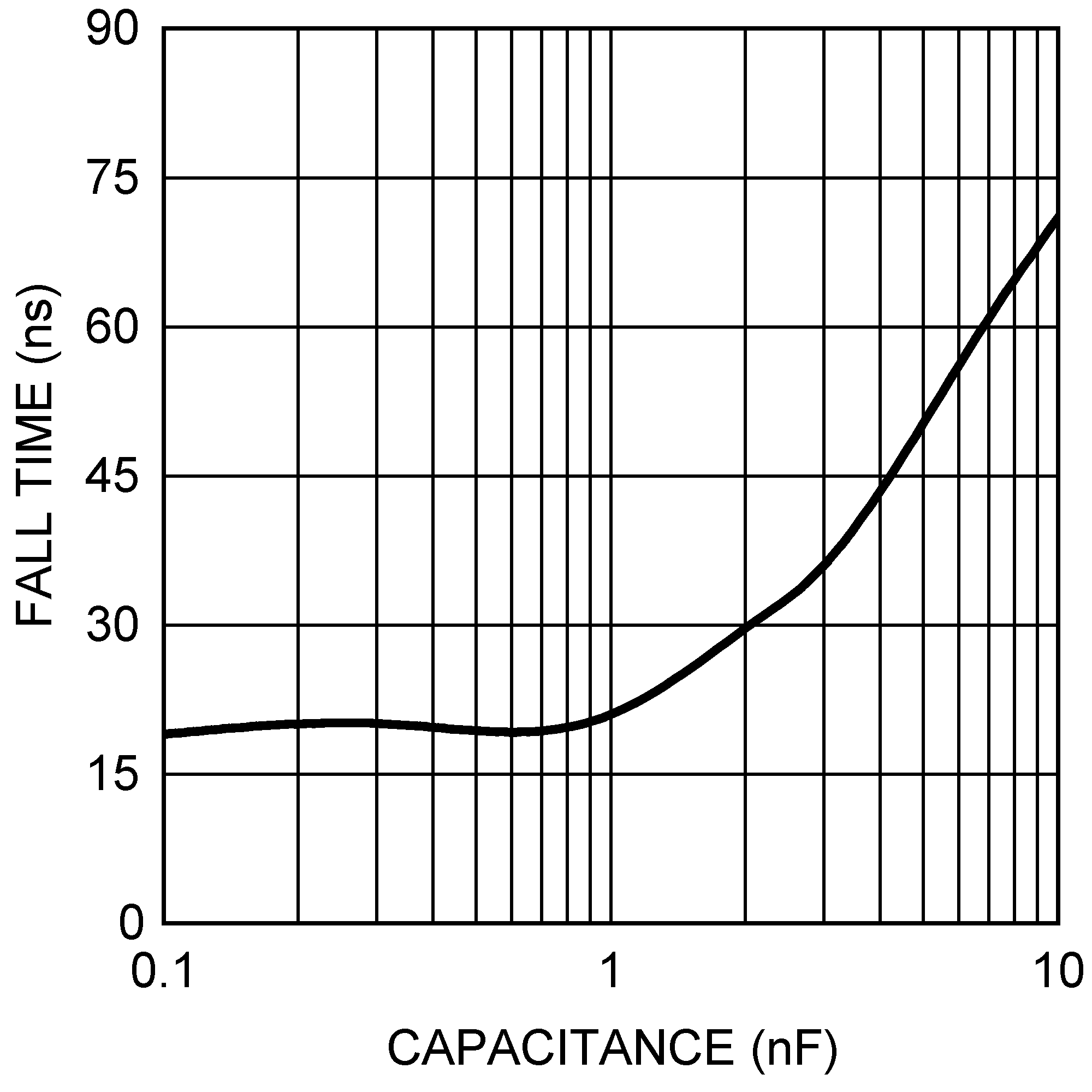
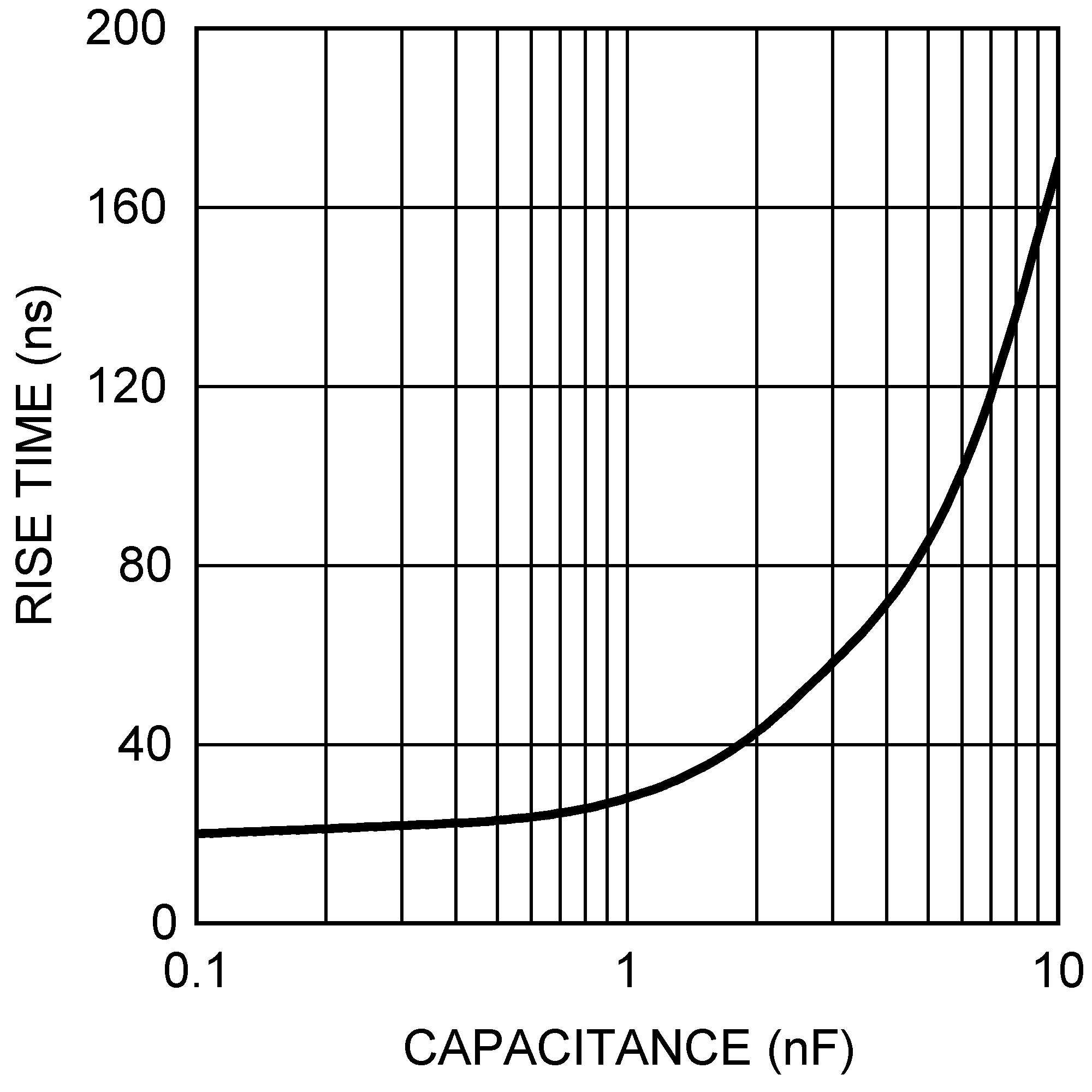
| tRISE | OUT Pin Rise Time | OUT Pin load = 1 nF | 18 | ns | ||
| tFALL | OUT Pin Fall Time | OUT Pin load = 1 nF | 15 | ns | ||
| THERMAL CHARACTERISTICS | ||||||
| TSD | Thermal Shutdown Threshold | 165 | °C | |||
| TSD-HYS | Thermal Shutdown Hysteresis | 25 | °C | |||
(1) All minimum and maximum limits are specified by correlating the electrical characteristics to process and temperature variations and applying statistical process control. The junction temperature (TJ in °C) is calculated from the ambient temperature (TA in °C) and power dissipation (PD in Watts) as follows: TJ = TA + (PD • RθJA) where RθJA (in °C/W) is the package thermal impedance provided in the Thermal Information section.
(2) VCC provides bias for the internal gate drive and control circuits.
(3) Device thermal limitations may limit usable range.
(4) Specification applies to the oscillator frequency.
6.6 Typical Characteristics
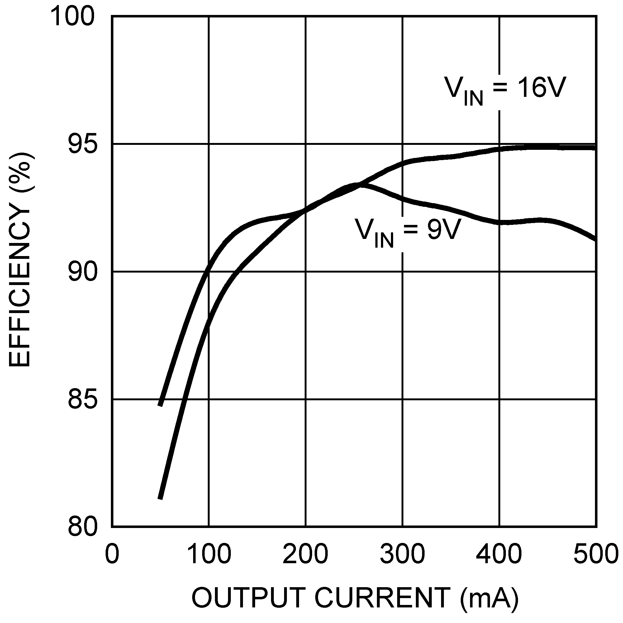
| VO = 40 V |
| TA = 25°C |
| TA = 25°C |

| RT = 6.65 KΩ | ||

| TA = 25°C |
| VIN = 24 V |
| TA = 25°C |
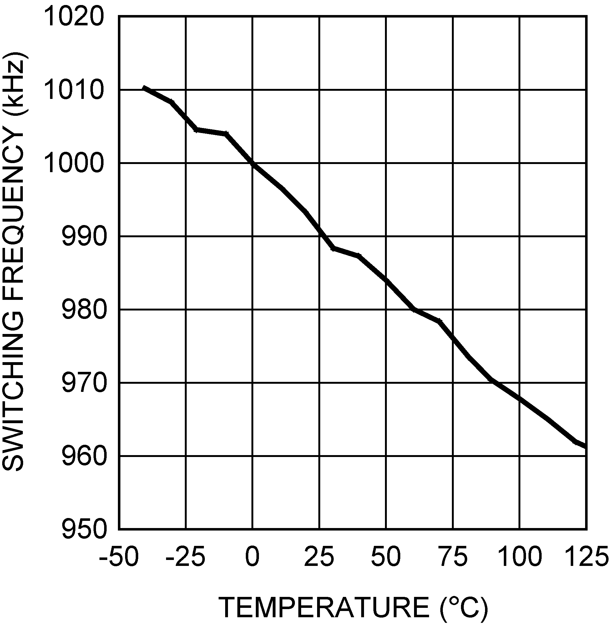
| RT = 16.2 KΩ |
