ZHCSES8 March 2016 LM5022-Q1
PRODUCTION DATA.
- 1 特性
- 2 应用
- 3 说明
- 4 修订历史记录
- 5 Pin Configuration and Functions
- 6 Specifications
- 7 Detailed Description
-
8 Application and Implementation
- 8.1 Application Information
- 8.2
Typical Application
- 8.2.1 Design Requirements
- 8.2.2
Detailed Design Procedure
- 8.2.2.1 Switching Frequency
- 8.2.2.2 MOSFET
- 8.2.2.3 Output Diode
- 8.2.2.4 Boost Inductor
- 8.2.2.5 Output Capacitor
- 8.2.2.6 VCC Decoupling Capacitor
- 8.2.2.7 Input Capacitor
- 8.2.2.8 Current Sense Filter
- 8.2.2.9 RSNS, RS2 and Current Limit
- 8.2.2.10 Control Loop Compensation
- 8.2.2.11 Efficiency Calculations
- 8.2.3 Application Curves
- 9 Power Supply Recommendations
- 10Layout
- 11器件和文档支持
- 12机械、封装和可订购信息
8 Application and Implementation
NOTE
Information in the following applications sections is not part of the TI component specification, and TI does not warrant its accuracy or completeness. TI’s customers are responsible for determining suitability of components for their purposes. Customers should validate and test their design implementation to confirm system functionality.
8.1 Application Information
The most common circuit controlled by the LM5022-Q1 is a non-isolated boost regulator. The boost regulator steps up the input voltage and has a duty ratio D of:

where
- VD is the forward voltage drop of the output diode
The following is a design procedure for selecting all the components for the boost converter circuit shown in Figure 15. The application is "in-cabin" automotive, meaning that the operating ambient temperature ranges from –20°C to 85°C. This circuit operates in continuous conduction mode (CCM), where inductor current stays above 0 A at all times, and delivers an output voltage of 40 V ±2% at a maximum output current of 0.5A. Additionally, the regulator must be able to handle a load transient of up to 0.5 A while keeping VO within ±4%. The voltage input comes from the battery/alternator system of an automobile, where the standard range 9 V to 16 V and transients of up to 32 V must not cause any malfunction.
8.2 Typical Application
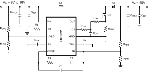 Figure 15. LM5022-Q1 Typical Application
8.2.1 Design Requirements
For typical low-side controller applications, use the parameters listed in Table 1.
Table 1. Design Parameters
| DESIGN PARAMETER | EXAMPLE VALUE |
|---|---|
| Minimum input voltage | 9 V to 16 V |
| Minimum output voltage | 40 V |
| Output current | 500 mA |
| Switching frequency | 500 kHz |
Table 2. BOM for Example Circuit
| ID | PART NUMBER | TYPE | SIZE | PARAMETERS | QTY | VENDOR |
|---|---|---|---|---|---|---|
| U1 | LM5022-Q1 | Low-Side Controller | 10-pin VSSOP | 60V | 1 | TI |
| Q1 | Si4850EY | MOSFET | SO-8 | 60V, 31mΩ, 27nC | 1 | Vishay |
| D1 | CMSH2-60M | Schottky Diode | SMA | 60V, 2A | 1 | Central Semi |
| L1 | SLF12575T-M3R2 | Inductor | 12.5 x 12.5 x 7.5 mm | 33µH, 3.2A, 40mΩ | 1 | TDK |
| Cin1, Cin2 | C4532X7R1H475M | Capacitor | 1812 | 4.7µF, 50V, 3mΩ | 2 | TDK |
| Co1, Co2 | C5750X7R2A475M | Capacitor | 2220 | 4.7µF,100V, 3mΩ | 2 | TDK |
| Cf | C2012X7R1E105K | Capacitor | 0805 | 1µF, 25V | 1 | TDK |
| Cinx Cox |
C2012X7R2A104M | Capacitor | 0805 | 100nF, 100V | 2 | TDK |
| C1 | VJ0805A561KXXAT | Capacitor | 0805 | 560pF 10% | 1 | Vishay |
| C2 | VJ0805Y124KXXAT | Capacitor | 0805 | 120nF 10% | 1 | Vishay |
| Css | VJ0805Y103KXXAT | Capacitor | 0805 | 10nF 10% | 1 | Vishay |
| Ccs | VJ0805Y102KXXAT | Capacitor | 0805 | 1nF 10% | 1 | Vishay |
| R1 | CRCW08053011F | Resistor | 0805 | 3.01kΩ 1% | 1 | Vishay |
| Rfb1 | CRCW08056490F | Resistor | 0805 | 649Ω 1% | 1 | Vishay |
| Rfb2 | CRCW08052002F | Resistor | 0805 | 20kΩ 1% | 1 | Vishay |
| Rs1 | CRCW0805101J | Resistor | 0805 | 100Ω 5% | 1 | Vishay |
| Rs2 | CRCW08053571F | Resistor | 0805 | 3.57kΩ 1% | 1 | Vishay |
| Rsns | ERJL14KF10C | Resistor | 1210 | 100mΩ, 1%, 0.5W | 1 | Panasonic |
| Rt | CRCW08053322F | Resistor | 0805 | 33.2kΩ 1% | 1 | Vishay |
| Ruv1 | CRCW08052611F | Resistor | 0805 | 2.61kΩ 1% | 1 | Vishay |
| Ruv2 | CRCW08051002F | Resistor | 0805 | 10kΩ 1% | 1 | Vishay |
8.2.2 Detailed Design Procedure
8.2.2.1 Switching Frequency
The selection of switching frequency is based on the tradeoffs between size, cost, and efficiency. In general, a lower frequency means larger, more expensive inductors and capacitors will be needed. A higher switching frequency generally results in a smaller but less efficient solution, as the power MOSFET gate capacitances must be charged and discharged more often in a given amount of time. For this application, a frequency of 500 kHz was selected as a good compromise between the size of the inductor and efficiency. PCB area and component height are restricted in this application. Following the equation given for RT in Equation 1, a 33.2-kΩ 1% resistor should be used to switch at 500 kHz.
8.2.2.2 MOSFET
Selection of the power MOSFET is governed by tradeoffs between cost, size, and efficiency. Breaking down the losses in the MOSFET is one way to determine relative efficiencies between different devices. For this example, the SO-8 package provides a balance of a small footprint with good efficiency.
Losses in the MOSFET can be broken down into conduction loss, gate charging loss, and switching loss.
Conduction, or I2R loss, PC, is approximately:

The factor 1.3 accounts for the increase in MOSFET on resistance due to heating. Alternatively, the factor of 1.3 can be ignored and the maximum on resistance of the MOSFET can be used.
Gate charging loss, PG, results from the current required to charge and discharge the gate capacitance of the power MOSFET and is approximated as:
QG is the total gate charge of the MOSFET. Gate charge loss differs from conduction and switching losses because the actual dissipation occurs in the LM5022-Q1 and not in the MOSFET itself. If no external bias is applied to the VCC pin, additional loss in the LM5022-Q1 IC occurs as the MOSFET driving current flows through the VCC regulator. This loss, PVCC, is estimated as:
Switching loss, PSW, occurs during the brief transition period as the MOSFET turns on and off. During the transition period both current and voltage are present in the channel of the MOSFET. The loss can be approximated as:
where
- tR is the rise time of the MOSFET
- tF is the fall time of the MOSFET
For this example, the maximum drain-to-source voltage applied across the MOSFET is VO plus the ringing due to parasitic inductance and capacitance. The maximum drive voltage at the gate of the high side MOSFET is VCC, or 7 V typical. The MOSFET selected must be able to withstand 40V plus any ringing from drain to source, and be able to handle at least 7V plus ringing from gate to source. A minimum voltage rating of 50VD-S and 10VG-S MOSFET will be used. Comparing the losses in a spreadsheet leads to a 60VD-S rated MOSFET in SO-8 with an RDSON of 22 mΩ (the maximum vallue is 31 mΩ), a gate charge of 27 nC, and rise and falls times of 10 ns and 12 ns, respectively.
8.2.2.3 Output Diode
The boost regulator requires an output diode D1 (see Figure 15) to carrying the inductor current during the MOSFET off-time. The most efficient choice for D1 is a Schottky diode due to low forward drop and near-zero reverse recovery time. D1 must be rated to handle the maximum output voltage plus any switching node ringing when the MOSFET is on. In practice, all switching converters have some ringing at the switching node due to the diode parasitic capacitance and the lead inductance. D1 must also be rated to handle the average output current, IO.
The overall converter efficiency becomes more dependent on the selection of D1 at low duty cycles, where the boost diode carries the load current for an increasing percentage of the time. This power dissipation can be calculating by checking the typical diode forward voltage, VD, from the I-V curve on the diode's datasheet and then multiplying it by IO. Diode datasheets will also provide a typical junction-to-ambient thermal resistance, RθJA, which can be used to estimate the operating die temperature of the Schottky. Multiplying the power dissipation (PD = IO × VD) by RθJA gives the temperature rise. The diode case size can then be selected to maintain the Schottky diode temperature below the operational maximum.
In this example a Schottky diode rated to 60 V and 1 A will be suitable, as the maximum diode current will be 0.5 A. A small case such as SOD-123 can be used if a small footprint is critical. Larger case sizes generally have lower RθJA and lower forward voltage drop, so for better efficiency the larger SMA case size will be used.
8.2.2.4 Boost Inductor
The first criterion for selecting an inductor is the inductance itself. In fixed-frequency boost converters this value is based on the desired peak-to-peak ripple current, ΔiL, which flows in the inductor along with the average inductor current, IL. For a boost converter in CCM IL is greater than the average output current, IO. The two currents are related by the following expression:
As with switching frequency, the inductance used is a tradeoff between size and cost. Larger inductance means lower input ripple current, however because the inductor is connected to the output during the off-time only there is a limit to the reduction in output ripple voltage. Lower inductance results in smaller, less expensive magnetics. An inductance that gives a ripple current of 30% to 50% of IL is a good starting point for a CCM boost converter. Minimum inductance should be calculated at the extremes of input voltage to find the operating condition with the highest requirement:

By calculating in terms of amperes, volts, and megahertz, the inductance value will come out in micro henries.
In order to ensure that the boost regulator operates in CCM a second equation is needed, and must also be evaluated at the corners of input voltage to find the minimum inductance required:

By calculating in terms of volts, amps and megahertz the inductance value will come out in µH.
For this design ΔiL will be set to 40% of the maximum IL. Duty cycle is evaluated first at VIN(MIN) and at VIN(MAX). Second, the average inductor current is evaluated at the two input voltages. Third, the inductor ripple current is determined. Finally, the inductance can be calculated, and a standard inductor value selected that meets all the criteria.
- Inductance for Minimum Input Voltage
- Inductance for Maximum Input Voltage


Maximum average inductor current occurs at VIN(MIN), and the corresponding inductor ripple current is 0.92 AP-P. Selecting an inductance that exceeds the ripple current requirement at VIN(MIN) and the requirement to stay in CCM for VIN(MAX) provides a tradeoff that allows smaller magnetics at the cost of higher ripple current at maximum input voltage. For this example, a 33-µH inductor will satisfy these requirements.
The second criterion for selecting an inductor is the peak current carrying capability. This is the level above which the inductor will saturate. In saturation the inductance can drop off severely, resulting in higher peak current that may overheat the inductor or push the converter into current limit. In a boost converter, peak current, IPK, is equal to the maximum average inductor current plus one half of the ripple current. First, the current ripple must be determined under the conditions that give maximum average inductor current:

Maximum average inductor current occurs at VIN(MIN). Using the selected inductance of 33 µH yields the following:
The highest peak inductor current over all operating conditions is therefore:
Hence an inductor must be selected that has a peak current rating greater than 2.5 A and an average current rating greater than 2.3A. One possibility is an off-the-shelf 33 µH ±20% inductor that can handle a peak current of 3.2 A and an average current of 3.4 A. Finally, the inductor current ripple is recalculated at the maximum input voltage:
8.2.2.5 Output Capacitor
The output capacitor in a boost regulator supplies current to the load during the MOSFET on-time and also filters the AC portion of the load current during the off-time. This capacitor determines the steady state output voltage ripple, ΔVO, a critical parameter for all voltage regulators. Output capacitors are selected based on their capacitance, CO, their equivalent series resistance (ESR) and their RMS or AC current rating.
The magnitude of ΔVO is comprised of three parts, and in steady state the ripple voltage during the on-time is equal to the ripple voltage during the off-time. For simplicity the analysis will be performed for the MOSFET turning off (off-time) only. The first part of the ripple voltage is the surge created as the output diode D1 turns on. At this point inductor/diode current is at the peak value, and the ripple voltage increase can be calculated as:
The second portion of the ripple voltage is the increase due to the charging of CO through the output diode. This portion can be approximated as:
The final portion of the ripple voltage is a decrease due to the flow of the diode/inductor current through the output capacitor’s ESR. This decrease can be calculated as:
The total change in output voltage is then:
The combination of two positive terms and one negative term may yield an output voltage ripple with a net rise or a net fall during the converter off-time. The ESR of the output capacitor(s) has a strong influence on the slope and direction of ΔVO. Capacitors with high ESR such as tantalum and aluminum electrolytic create an output voltage ripple that is dominated by ΔVO1 and ΔVO3, with a shape shown in Figure 16. Ceramic capacitors, in contrast, have very low ESR and lower capacitance. The shape of the output ripple voltage is dominated by ΔVO2, with a shape shown in Figure 17.
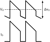 Figure 16. ΔVO Using High ESR Capacitors
 Figure 17. ΔVO Using Low ESR Capacitors
For this example the small size and high temperature rating of ceramic capacitors make them a good choice. The output ripple voltage waveform of Figure 17 is assumed, and the capacitance will be selected first. The desired ΔVO is ±2% of 40V, or 0.8VP-P. Beginning with the calculation for ΔVO2, the required minimum capacitance is:
The next higher standard 20% capacitor value is 1 µF, however to provide margin for component tolerance and load transients two capacitors rated 4.7 µF each will be used. Ceramic capacitors rated 4.7 µF ±20% are available from many manufacturers. The minimum quality dielectric that is suitable for switching power supply output capacitors is X5R, while X7R (or better) is preferred. Careful attention must be paid to the DC voltage rating and case size, as ceramic capacitors can lose 60% or more of their rated capacitance at the maximum DC voltage. This is the reason that ceramic capacitors are often de-rated to 50% of their capacitance at their working voltage. The output capacitors for this example will have a 100V rating in a 2220 case size.
The typical ESR of the selected capacitors is 3 mΩ each, and in parallel is approximately 1.5 mΩ. The worst-case value for ΔVO1 occurs during the peak current at minimum input voltage:
The worst-case capacitor charging ripple occurs at maximum duty cycle:
Finally, the worst-case value for ΔVO3 occurs when inductor ripple current is highest, at maximum input voltage:
The output voltage ripple can be estimated by summing the three terms:
The RMS current through the output capacitor(s) can be estimated using the following, worst-case equation:

The highest RMS current occurs at minimum input voltage. For this example the maximum output capacitor RMS current is:
These 2220 case size devices are capable of sustaining RMS currents of over 3A each, making them more than adequate for this application.
8.2.2.6 VCC Decoupling Capacitor
The VCC pin should be decoupled with a ceramic capacitor placed as close as possible to the VCC and GND pins of the LM5022-Q1. The decoupling capacitor should have a minimum X5R or X7R type dielectric to ensure that the capacitance remains stable over voltage and temperature, and be rated to a minimum of 470 nF. One good choice is a 1-µF device with X7R dielectric and 1206 case size rated to 25 V.
8.2.2.7 Input Capacitor
The input capacitors to a boost regulator control the input voltage ripple, ΔVIN, hold up the input voltage during load transients, and prevent impedance mismatch (also called power supply interaction) between the LM5022-Q1 and the inductance of the input leads. Selection of input capacitors is based on their capacitance, ESR, and RMS current rating. The minimum value of ESR can be selected based on the maximum output current transient, ISTEP, using the following expression:

For this example the maximum load step is equal to the load current, or 0.5A. The maximum permissible ΔVIN during load transients is 4%P-P. ΔVIN and duty cycle are taken at minimum input voltage to give the worst-case value:
The minimum input capacitance can be selected based on ΔVIN, based on the drop in VIN during a load transient, or based on prevention of power supply interaction. In general, the requirement for greatest capacitance comes from the power supply interaction. The inductance and resistance of the input source must be estimated, and if this information is not available, they can be assumed to be 1 µH and 0.1 Ω, respectively. Minimum capacitance is then estimated as:

As with ESR, the worst-case, highest minimum capacitance calculation comes at the minimum input voltage. Using the default estimates for LS and RS, minimum capacitance is:

The next highest standard 20% capacitor value is 6.8 µF, but because the actual input source impedance and resistance are not known, two 4.7 µF capacitors will be used. In general, doubling the calculated value of input capacitance provides a good safety margin. The final calculation is for the RMS current. For boost converters operating in CCM this can be estimated as:
From the inductor section, maximum inductor ripple current is 0.58 A, hence the input capacitor(s) must be rated to handle 0.29 × 0.58 = 170 mARMS.
The input capacitors can be ceramic, tantalum, aluminum, or almost any type, however the low capacitance requirement makes ceramic capacitors particularly attractive. As with the output capacitors, the minimum quality dielectric used should X5R, with X7R or better preferred. The voltage rating for input capacitors need not be as conservative as the output capacitors, as the need for capacitance decreases as input voltage increases. For this example, the capacitor selected will be 4.7 µF ±20%, rated to 50 V, in the 1812 case size. The RMS current rating of these capacitors is over 2A each, more than enough for this application.
8.2.2.8 Current Sense Filter
Parasitic circuit capacitance, inductance and gate drive current create a spike in the current sense voltage at the point where Q1 turns on. In order to prevent this spike from terminating the on-time prematurely, every circuit should have a low-pass filter that consists of CCS and RS1, shown in Figure 15. The time constant of this filter should be long enough to reduce the parasitic spike without significantly affecting the shape of the actual current sense voltage. The recommended range for RS1 is between 10 Ω and 500 Ω, and the recommended range for CCS is between 100 pF and 2.2 nF. For this example, the values of RS1 and CCS will be 100Ω and 1 nF, respectively.
8.2.2.9 RSNS, RS2 and Current Limit
The current sensing resistor RSNS is used for steady state regulation of the inductor current and to sense overcurrent conditions. The slope compensation resistor is used to ensure control loop stability, and both resistors affect the current limit threshold. The RSNS value selected must be low enough to keep the power dissipation to a minimum, yet high enough to provide good signal-to-noise ratio for the current sensing circuitry. RSNS, and RS2 should be set so that the current limit comparator, with a threshold of 0.5 V, trips before the sensed current exceeds the peak current rating of the inductor, without limiting the output power in steady state.
For this example the peak current, at VIN(MIN), is 2.5 A, while the inductor itself is rated to 3.2 A. The threshold for current limit, ILIM, is set slightly between these two values to account for tolerance of the circuit components, at a level of 3 A. The required resistor calculation must take into account both the switch current through RSNS and the compensation ramp current flowing through the internal 2 kΩ, RS1 and RS2 resistors. RSNS should be selected first because it is a power resistor with more limited selection. The following equation should be evaluated at VIN(MIN), when duty cycle is highest:


where
- L is in µH
- fSW in MHz
The closest 5% value is 100 mΩ. Power dissipation in RSNS can be estimated by calculating the average current. The worst-case average current through RSNS occurs at minimum input voltage/maximum duty cycle and can be calculated as:

For this example a 0.1 Ω ±1%, thick-film chip resistor in a 1210 case size rated to 0.5W will be used.
With RSNS selected, RS2 can be determined using the following expression:


The closest 1% tolerance value is 3.57 kΩ.
8.2.2.10 Control Loop Compensation
The LM5022-Q1 uses peak current-mode PWM control to correct changes in output voltage due to line and load transients. Peak current-mode provides inherent cycle-by-cycle current limiting, improved line transient response, and easier control loop compensation.
The control loop is comprised of two parts. The first is the power stage, which consists of the pulse width modulator, output filter, and the load. The second part is the error amplifier, which is an op-amp configured as an inverting amplifier. Figure 18 shows the regulator control loop components.
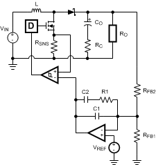 Figure 18. Power Stage and Error Amplifier
One popular method for selecting the compensation components is to create Bode plots of gain and phase for the power stage and error amplifier. Combined, they make the overall bandwidth and phase margin of the regulator easy to determine. Software tools such as Excel, MathCAD, and Matlab are useful for observing how changes in compensation or the power stage affect system gain and phase.
The power stage in a CCM peak current mode boost converter consists of the DC gain, APS, a single low frequency pole, ƒLFP, the ESR zero, ƒZESR, a right-half plane zero, ƒRHP, and a double pole resulting from the sampling of the peak current. The power stage transfer function (also called the Control-to-Output transfer function) can be written:
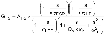
where
- the DC gain is defined as:

where
The system ESR zero is:

The low frequency pole is:

The right-half plane zero is:

The sampling double pole quality factor is:

The sampling double corner frequency is:
The natural inductor current slope is:
The external ramp slope is:
In the equation for APS, DC gain is highest when input voltage and output current are at the maximum. In this the example those conditions are VIN = 16 V and IO = 500 mA.
DC gain is 44 dB. The low frequency pole fP = 2πωP is at 423 Hz, the ESR zero fZ = 2πωZ is at 5.6 MHz, and the right-half plane zero ƒRHP = 2πωRHP is at 61 kHz. The sampling double-pole occurs at one-half of the switching frequency. Proper selection of slope compensation (via RS2) is most evident the sampling double pole. A well-selected RS2 value eliminates peaking in the gain and reduces the rate of change of the phase lag. Gain and phase plots for the power stage are shown in Figure 19 and Figure 20.
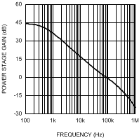 Figure 19. Power Stage Gain and Phase
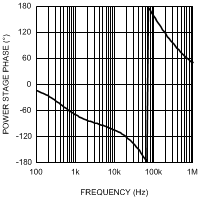 Figure 20. Power Stage Gain and Phase
The single pole causes a roll-off in the gain of –20 dB/decade at lower frequency. The combination of the RHP zero and sampling double pole maintain the slope out to beyond the switching frequency. The phase tends towards –90° at lower frequency but then increases to –180° and beyond from the RHP zero and the sampling double pole. The effect of the ESR zero is not seen because its frequency is several decades above the switching frequency. The combination of increasing gain and decreasing phase makes converters with RHP zeroes difficult to compensate. Setting the overall control loop bandwidth to 1/3 to 1/10 of the RHP zero frequency minimizes these negative effects, but requires a compromise in the control loop bandwidth. If this loop were left uncompensated, the bandwidth would be 89 kHz and the phase margin -54°. The converter would oscillate, and therefore is compensated using the error amplifier and a few passive components.
The transfer function of the compensation block, GEA, can be derived by treating the error amplifier as an inverting op-amp with input impedance ZI and feedback impedance ZF. The majority of applications will require a Type II, or two-pole one-zero amplifier, shown in Figure 18. The LaPlace domain transfer function for this Type II network is given by the following:

Many techniques exist for selecting the compensation component values. The following method is based upon setting the mid-band gain of the error amplifier transfer function first and then positioning the compensation zero and pole:
- Determine the desired control loop bandwidth: The control loop bandwidth, ƒ0dB, is the point at which the total control loop gain (H = GPS × GEA) is equal to 0 dB. For this example, a low bandwidth of 10 kHz, or approximately 1/6th of the RHP zero frequency, is chosen because of the wide variation in input voltage.
- Determine the gain of the power stage at ƒ0dB: This value, A, can be read graphically from the gain plot of GPS or calculated by replacing the ‘s’ terms in GPS with ‘2 πf0dB’. For this example the gain at 10 kHz is approximately 16 dB.
- Calculate the negative of A and convert it to a linear gain: By setting the mid-band gain of the error amplifier to the negative of the power stage gain at f0dB, the control loop gain will equal 0 dB at that frequency. For this example, –16 dB = 0.15V/V.
- Select the resistance of the top feedback divider resistor RFB2: This value is arbitrary, however selecting a resistance between 10 kΩ and 100 kΩ will lead to practical values of R1, C1 and C2. For this example, RFB2 = 20 kΩ 1%.
- Set R1 = A × RFB2: For this example: R1 = 0.15 × 20000 = 3 kΩ
- Select a frequency for the compensation zero, ƒZ1: The suggested placement for this zero is at the low frequency pole of the power stage, ƒLFP = ωLFP / 2π. For this example, ƒZ1 = ƒLFP = 423 Hz
-
Set

For this example, C2 = 125 nF - Select a frequency for the compensation pole, ƒP1: The suggested placement for this pole is at one-fifth of the switching frequency. For this example, ƒP1 = 100 kHz
-
Set

For this example, C1 = 530 pF -
Plug the closest 1% tolerance values for RFB2 and R1, then the closest 10% values for C1 and C2 into GEA and model the error amp: The open-loop gain and bandwidth of the LM5022-Q1’s internal error amplifier are 75 dB and 4 MHz, respectively. Their effect on GEA can be modeled using the following expression:

ADC is a linear gain, the linear equivalent of 75 dB is approximately 5600V/V. C1 = 560 pF 10%, C2 = 120 nF 10%, R1 = 3.01 kΩ 1% -
Plot or evaluate the actual error amplifier transfer function:

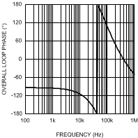
- Plot or evaluate the complete control loop transfer function: The complete control loop transfer function is obtained by multiplying the power stage and error amplifier functions together. The bandwidth and phase margin can then be read graphically or evaluated numerically. The bandwidth of this example circuit at VIN = 16 V is 10.5 kHz, with a phase margin of 66°.
- Re-evaluate at the corners of input voltage and output current: Boost converters exhibit significant change in their loop response when VIN and IO change. With the compensation fixed, the total control loop gain and phase should be checked to ensure a minimum phase margin of 45° over both line and load.

8.2.2.11 Efficiency Calculations
A reasonable estimation for the efficiency of a boost regulator controlled by the LM5022-Q1 can be obtained by adding together the loss is each current carrying element and using the equation:

The following shows an efficiency calculation to complement the circuit design from Device Functional Modes. Output power for this circuit is 40 V x 0.5 A = 20 W. Input voltage is assumed to be 13.8 V, and the calculations used assume that the converter runs in CCM. Duty cycle for VIN = 13.8V is 66%, and the average inductor current is 1.5 A.
8.2.2.11.1 Chip Operating Loss
This term accounts for the current drawn at the VIN pin. This current, IIN, drives the logic circuitry and the power MOSFETs. The gate driving loss term from MOSFET is included in the chip operating loss. For the LM5022-Q1, IIN is equal to the steady state operating current, ICC, plus the MOSFET driving current, IGC. Power is lost as this current passes through the internal linear regulator of the LM5022-Q1.
ICC is typically 3.5 mA, taken from the Electrical Characteristics table. Chip Operating Loss is then:
8.2.2.11.2 MOSFET Switching Loss
8.2.2.11.3 MOSFET and RSNS Conduction Loss
8.2.2.11.4 Output Diode Loss
The average output diode current is equal to IO, or 0.5 A. The estimated forward drop, VD, is 0.5 V. The output diode loss is therefore:
8.2.2.11.5 Input Capacitor Loss
This term represents the loss as input ripple current passes through the ESR of the input capacitor bank. In this equation ‘n’ is the number of capacitors in parallel. The 4.7 µF input capacitors selected have a combined ESR of approximately 1.5 mΩ, and ΔiL for a 13.8V input is 0.55A:

8.2.2.11.6 Output Capacitor Loss
This term is calculated using the same method as the input capacitor loss, substituting the output capacitor RMS current for VIN = 13.8 V. The output capacitors' combined ESR is also approximately 1.5 mΩ.
8.2.2.11.7 Boost Inductor Loss
The typical DCR of the selected inductor is 40 mΩ.
Core loss in the inductor is estimated to be equal to the DCR loss, adding an additional 90 mW to the total inductor loss.
8.2.2.11.8 Total Loss
8.2.2.11.9 Efficiency
8.2.3 Application Curves
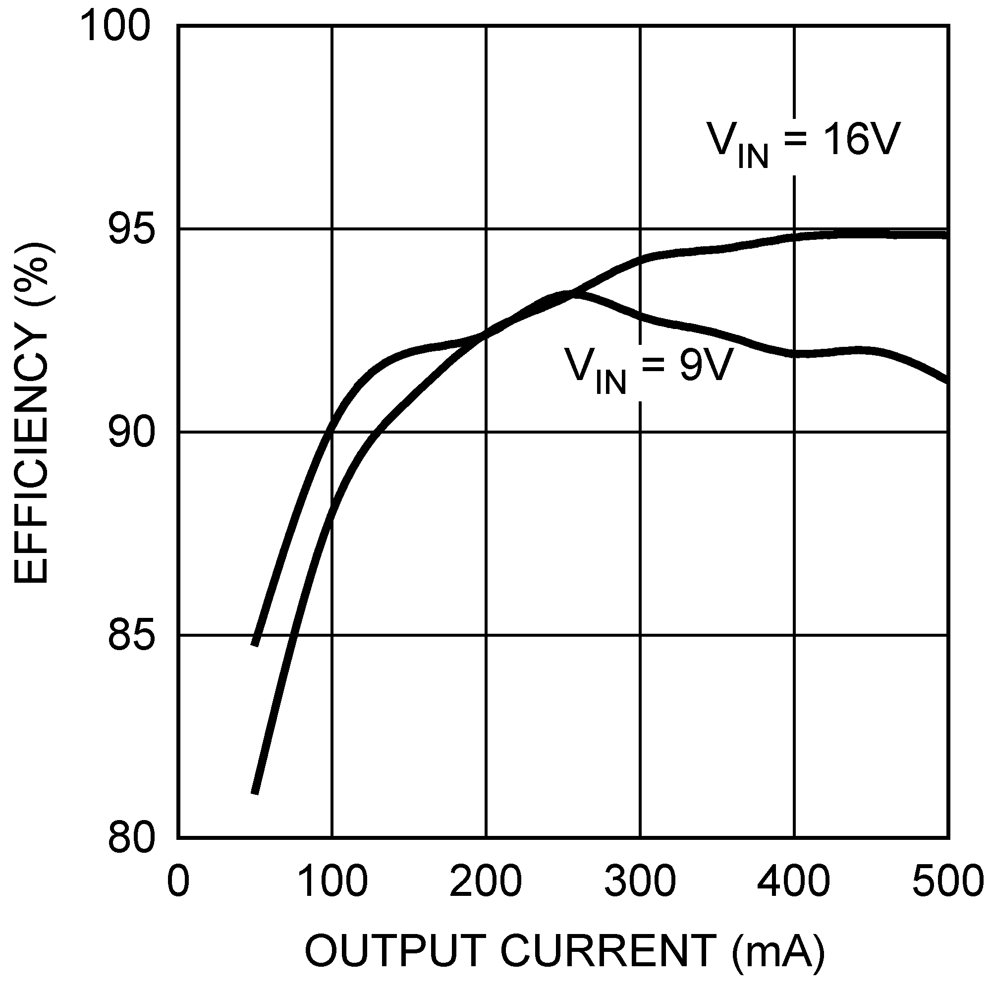
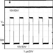
| VIN = 16-V | IO = 0.5-A |
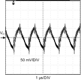
| VIN = 16-V | IO = 0.5-A |
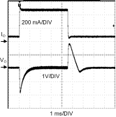
| VIN = 16-V | IO = 50mA - 500mA |
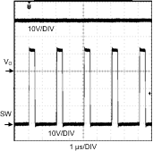
| VIN = 9-V | IO = 0.5-A |
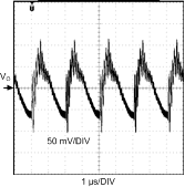
| VIN = 9-V | IO = 0.5-A | |
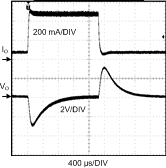
| VIN = 9-V | IO = 50mA - 500mA |