ZHCSKM9F May 2011 – December 2019 LM5050-1 , LM5050-1-Q1
PRODUCTION DATA.
- 1 特性
- 2 应用
- 3 说明
- 4 修订历史记录
- 5 Pin Configuration and Functions
- 6 Specifications
- 7 Detailed Description
-
8 Application and Implementation
- 8.1 Application Information
- 8.2
Typical Applications
- 8.2.1 Typical Application With Input and Output Transient Protection
- 8.2.2 Using a Separate VS Supply for Low Vin Operation
- 8.2.3 ORing of Two Power Sources
- 8.2.4 Reverse Input Voltage Protection With IQ Reduction
- 8.2.5 Basic Application With Input Transient Protection
- 8.2.6 48-V Application With Reverse Input Voltage (VIN = –48 V) Protection
- 9 Power Supply Recommendations
- 10Layout
- 11器件和文档支持
- 12机械、封装和可订购信息
8.1 Application Information
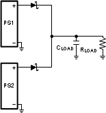
Systems that require high availability often use multiple, parallel-connected redundant power supplies to improve reliability. Schottky OR-ing diodes are typically used to connect these redundant power supplies to a common point at the load. The disadvantage of using OR-ing diodes is the forward voltage drop, which reduces the available voltage and the associated power losses as load currents increase. Using an N-channel MOSFET to replace the OR-ing diode requires a small increase in the level of complexity, but reduces, or eliminates, the need for diode heat sinks or large thermal copper area in circuit board layouts for high power applications.
 Figure 21. OR-ing with Diodes
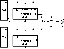
 The LM5050-1/-Q1 is a positive voltage (that is, high-side) OR-ing controller that will drive an external N-channel MOSFET to replace an OR-ing diode. The voltage across the MOSFET source and drain pins is monitored by the LM5050-1 at the IN and OUT pins, while the GATE pin drives the MOSFET to control its operation based on the monitored source-drain voltage. The resulting behavior is that of an ideal rectifier with source and drain pins of the MOSFET acting as the anode and cathode pins of a diode respectively.
 Figure 22. OR-ing With MOSFETs