SNVS628H October 2009 – December 2019 LM5060
PRODUCTION DATA.
- 1 Features
- 2 Applications
- 3 Description
- 4 Revision History
- 5 Pin Configuration and Functions
- 6 Specifications
- 7 Detailed Description
-
8 Application and Implementation
- 8.1 Application Information
- 8.2
Typical Applications
- 8.2.1
Example Number 1: LM5060EVAL Design
- 8.2.1.1 Design Requirements
- 8.2.1.2
Detailed Design Procedure
- 8.2.1.2.1 VDS Fault Detection and Selecting Sense Pin Resistor RS
- 8.2.1.2.2 Turn-On Time
- 8.2.1.2.3 Fault Detection Delay Time
- 8.2.1.2.4 MOSFET Selection
- 8.2.1.2.5 Input and Output Capacitors
- 8.2.1.2.6 UVLO, OVP
- 8.2.1.2.7 POWER GOOD Indicator
- 8.2.1.2.8 Input Bypass Capacitor
- 8.2.1.2.9 Large Load Capacitance
- 8.2.1.3 Application Curves
- 8.2.2 Example Number 2: Reverse Polarity Protection With Diodes
- 8.2.3 Example Number 3: Reverse Polarity Protection With Resistor
- 8.2.1
Example Number 1: LM5060EVAL Design
- 9 Power Supply Recommendations
- 10Layout
- 11Device and Documentation Support
- 12Mechanical, Packaging, and Orderable Information
8.2.1.2.6 UVLO, OVP
The UVLO and OVP thresholds are programmed to enable the external MOSFET (Q1) when the input supply voltage is within the desired operating range. If the supply voltage is low enough that the voltage at the UVLO pin is below the UVLO threshold, Q1 is switched off by a 2.2 mA (typical) current sink at the GATE pin, denying power to the load. The UVLO threshold has approximately 180 mV of hysteresis.
If the supply voltage is high enough that the voltage at the OVP pin is above the OVP threshold, the GATE pin is pulled low with a 80 mA current sink. Hysteresis is provided for each threshold. The OVP threshold has approximately 240 mV of hysteresis.
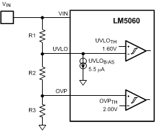
Option A: The configuration shown in Figure 29 requires three resistors (R1, R2, and R3) to set the thresholds.
 Figure 29. UVLO and OVP Thresholds Set by R1, R2 and R3
 The procedure to calculate the resistor values is as follows:
- Select R1 based on current consumption allowed in the resistor divider, including UVLOBIAS, and consideration of noise sensitivity. A value less than 100 kΩ is recommended, with lower values providing improved immunity to variations in ULVOBIAS.
- Calculate R3 with the following formula:
- Calculate R2 with the following formula:


VINMIN is the minimum and VINMAX is the maximum input voltage of the design specification. All other variables can be found in the Electrical Characteristics table of this document. To calculate the UVLO lower threshold including its hysteresis for falling VIN, use (UVLOTH-UVLOHYS) instead of UVLOTH in the formulas above. To calculate the OVP lower threshold including hysteresis for falling VIN, use (OVPTH-OVPHYS) instead of OVPTH. With three given resistors R1, R2, and R3, the thresholds can be calculated with the formulas below:

Also in these two formulas, the respective lower threshold value including the hysteresis is calculated by using (UVLOTH-UVLOHYS) instead of UVLOTH, and (OVPTH-OVPHYS) instead of OVPTH. The worst case thresholds, over the operating temperature range, can be calculated using the respective min and max values in bold font in the Electrical Characteristics.
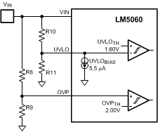
Option B: UVLO and OVP can be independently adjusted using two resistor dividers as shown in Figure 30.
 Figure 30. Programming the Thresholds with Resistors R8-R11
 Choose the upper UVLO thresholds to ensure operation down to the lowest required operating input voltage (VINMIN). Select R11 based on resistive divider current consumption and noise sensitivity. A value less than 100 kΩ is recommended, with lower values providing improved immunity to variations in ULVOBIAS.

To calculate the UVLO low threshold including its hysteresis, use (UVLOTH-UVLOHYS) instead of UVLOTH in the formula above. Choose the lower OVP threshold to ensure operation up to the highest VIN voltage required (VINMAX). Select R9 based on resistive divider current consumption A value less than 100 kΩ is recommended.

To calculate the OVP low threshold including hysteresis, use (OVPTH-OVPHYS) instead of OVPTH. Where the R9-R11 resistor values are known, the threshold voltages are calculated from the following:

Also in these two formulas, the respective low value including the threshold hysteresis is calculated by using (UVLOTH-UVLOHYS) instead of UVLOTH and (OVPTH-OVPHYS) instead of OVPTH. The worst case thresholds, over the operating temperature range, can be calculated using the respective minimum and maximum values in bold font in the Electrical Characteristics.
Option C: The OVP function can be disabled by grounding the OVP pin. The UVLO thresholds are set as described in Figure 30.