SNVS628H October 2009 – December 2019 LM5060
PRODUCTION DATA.
- 1 Features
- 2 Applications
- 3 Description
- 4 Revision History
- 5 Pin Configuration and Functions
- 6 Specifications
- 7 Detailed Description
-
8 Application and Implementation
- 8.1 Application Information
- 8.2
Typical Applications
- 8.2.1
Example Number 1: LM5060EVAL Design
- 8.2.1.1 Design Requirements
- 8.2.1.2
Detailed Design Procedure
- 8.2.1.2.1 VDS Fault Detection and Selecting Sense Pin Resistor RS
- 8.2.1.2.2 Turn-On Time
- 8.2.1.2.3 Fault Detection Delay Time
- 8.2.1.2.4 MOSFET Selection
- 8.2.1.2.5 Input and Output Capacitors
- 8.2.1.2.6 UVLO, OVP
- 8.2.1.2.7 POWER GOOD Indicator
- 8.2.1.2.8 Input Bypass Capacitor
- 8.2.1.2.9 Large Load Capacitance
- 8.2.1.3 Application Curves
- 8.2.2 Example Number 2: Reverse Polarity Protection With Diodes
- 8.2.3 Example Number 3: Reverse Polarity Protection With Resistor
- 8.2.1
Example Number 1: LM5060EVAL Design
- 9 Power Supply Recommendations
- 10Layout
- 11Device and Documentation Support
- 12Mechanical, Packaging, and Orderable Information
6.6 Typical Characteristics
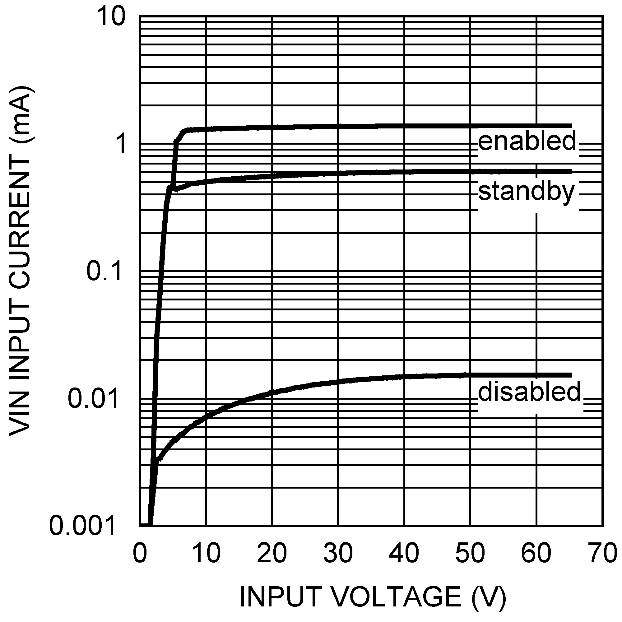 Figure 1. VIN Pin Current vs VIN Pin Voltage
  Figure 3. OUT Pin Current (IOUT-EN) vs VIN Voltage
 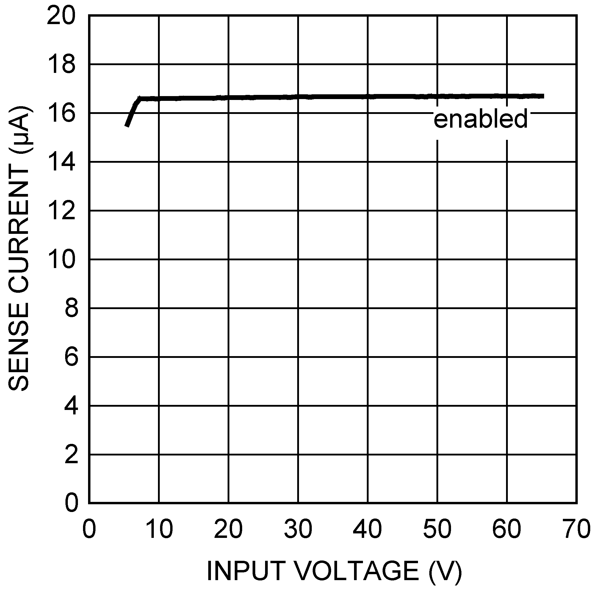 Figure 5. SENSE Current (ISENSE) vs VIN Voltage
 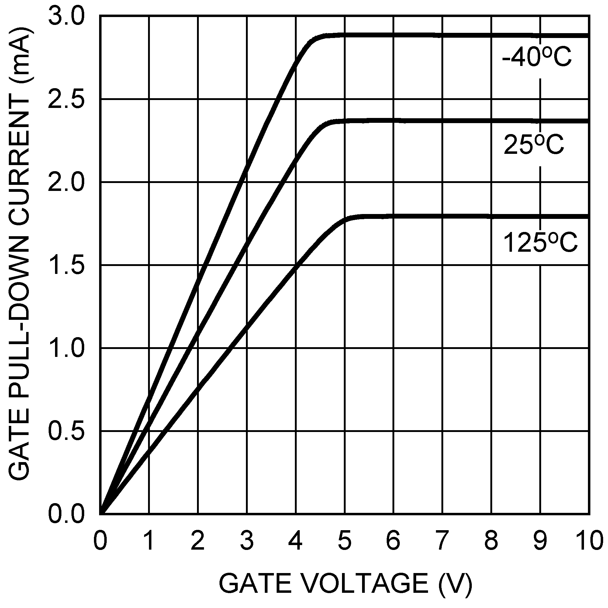 Figure 7. GATE Pull-Down Current Off (IGATE-OFF)
vs GATE Voltage
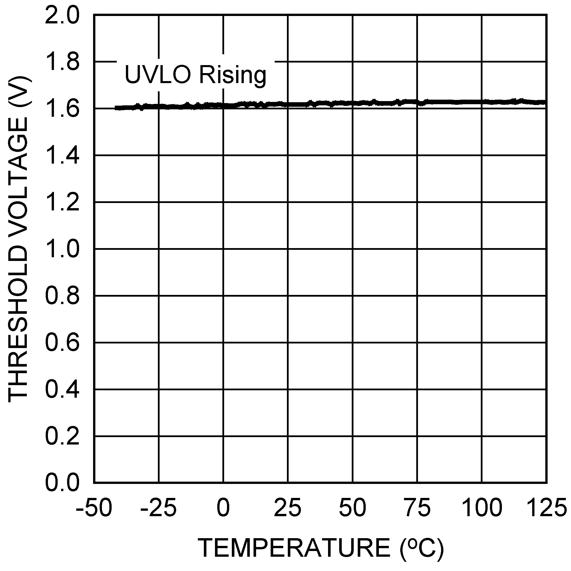 Figure 9. UVLO Threshold Voltage (UVLOTH)
vs Temperature
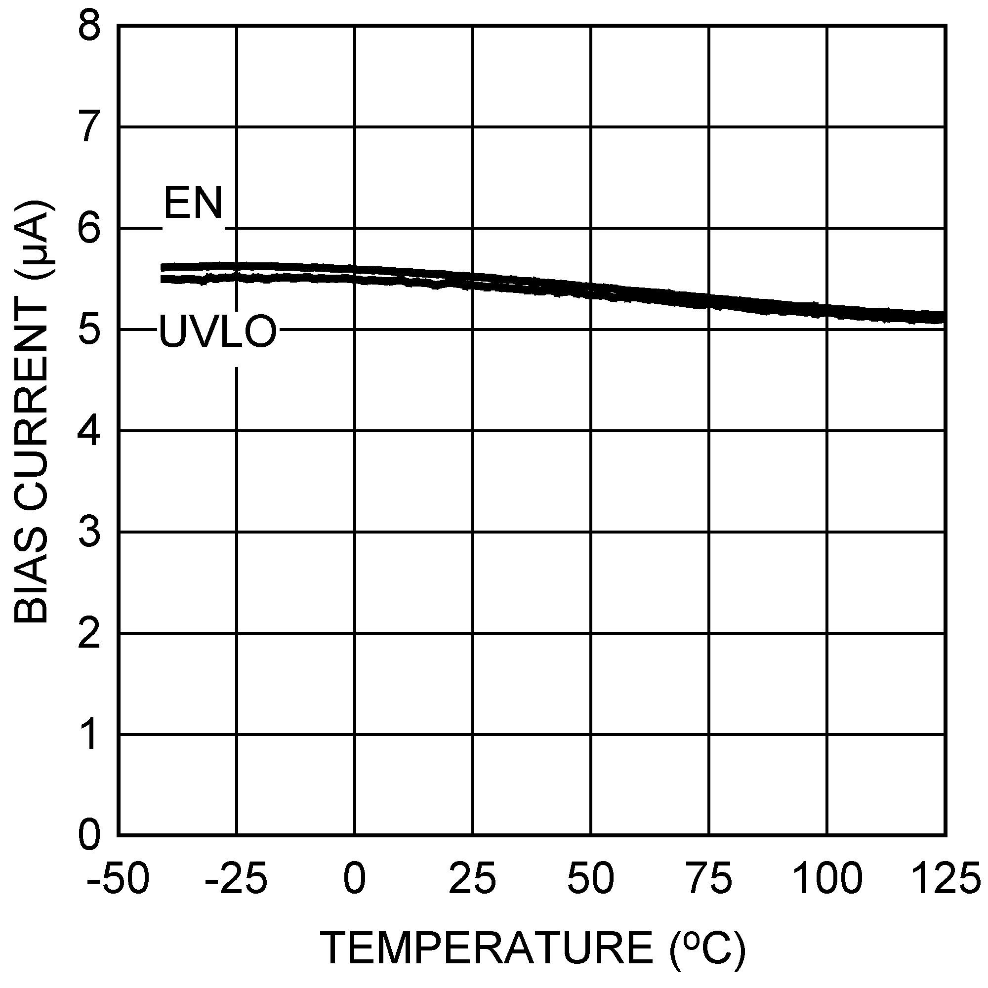 Figure 11. UVLO, EN Current vs Temperature
 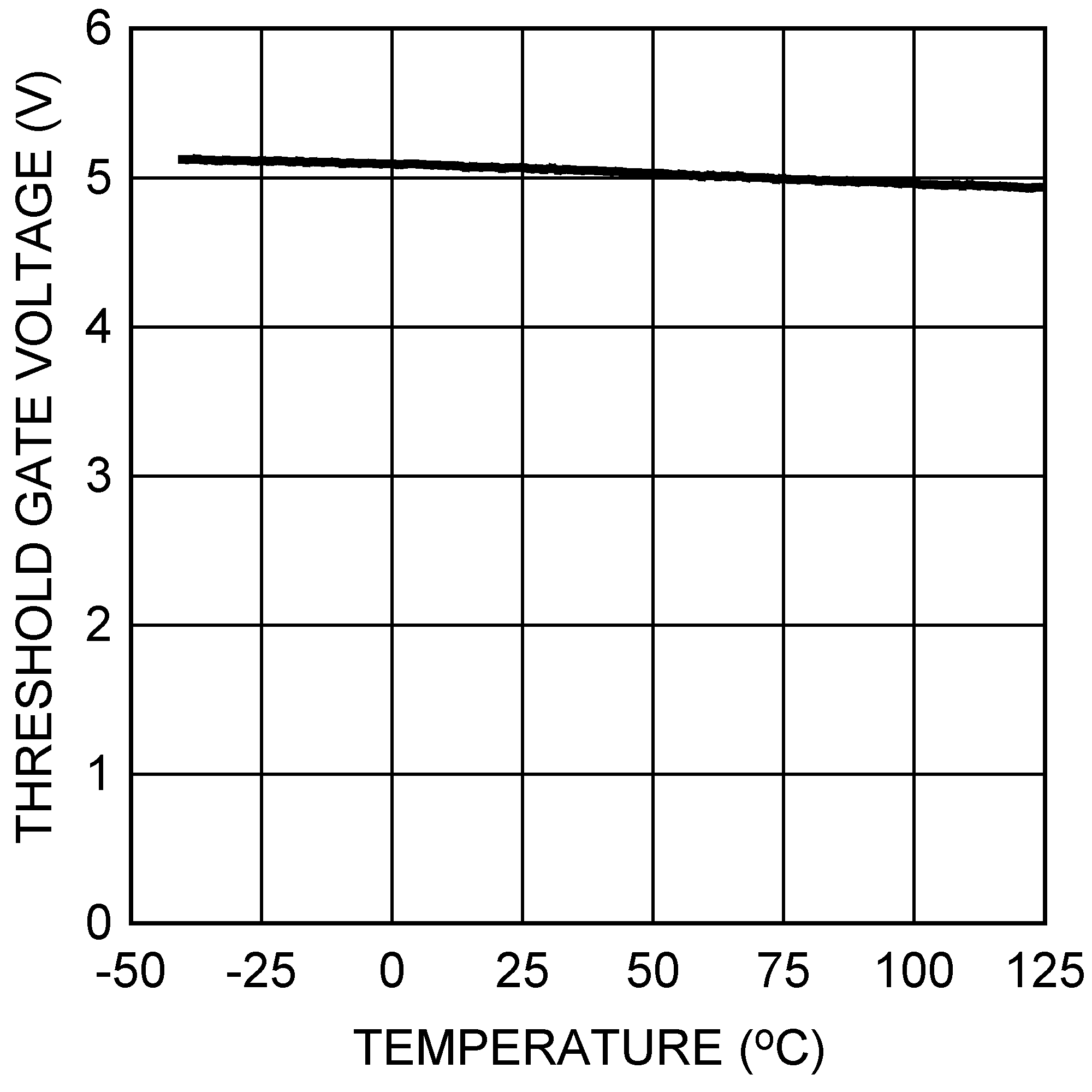 Figure 13. VGS Comparator Threshold Voltage (VGATE-TH)
vs Temperature
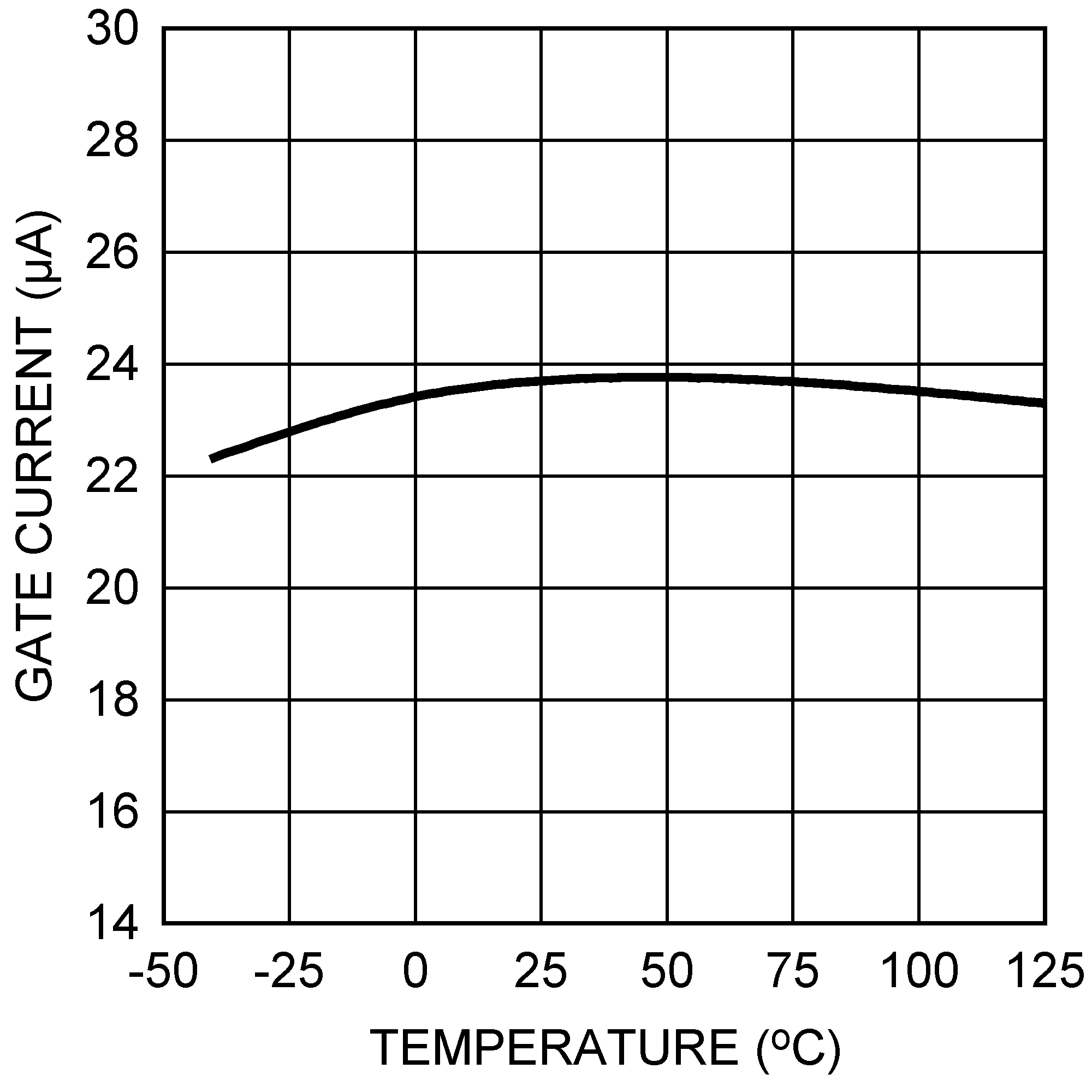 Figure 15. GATE Current (IGATE) vs Temperature
 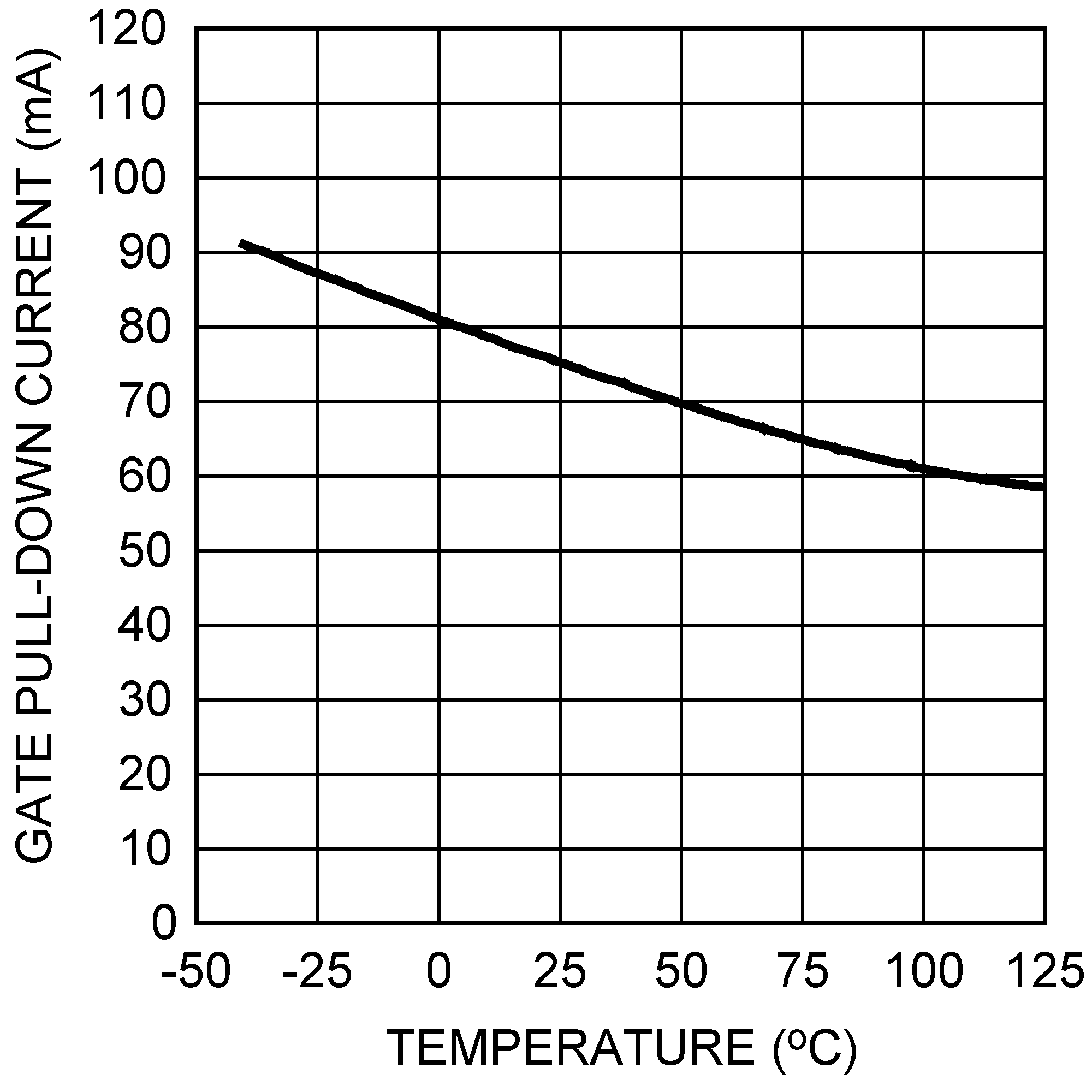 Figure 17. Gate Pull-Down Current - Fault (IGATE-FLT)
vs Temperature
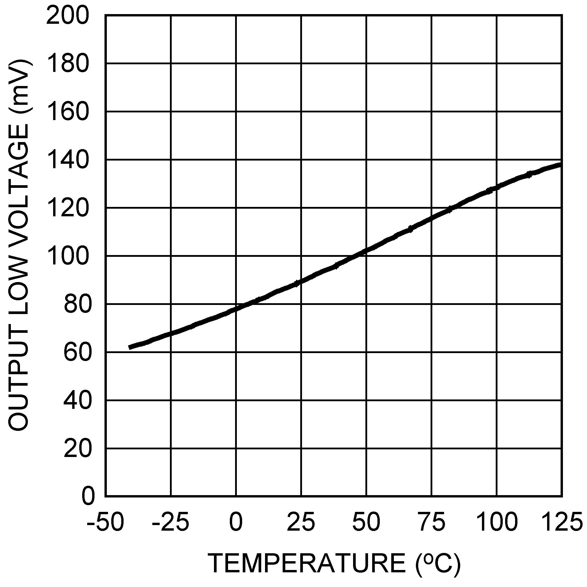 Figure 19. nPGD Low Voltage (PGDVOL) vs Temperature
 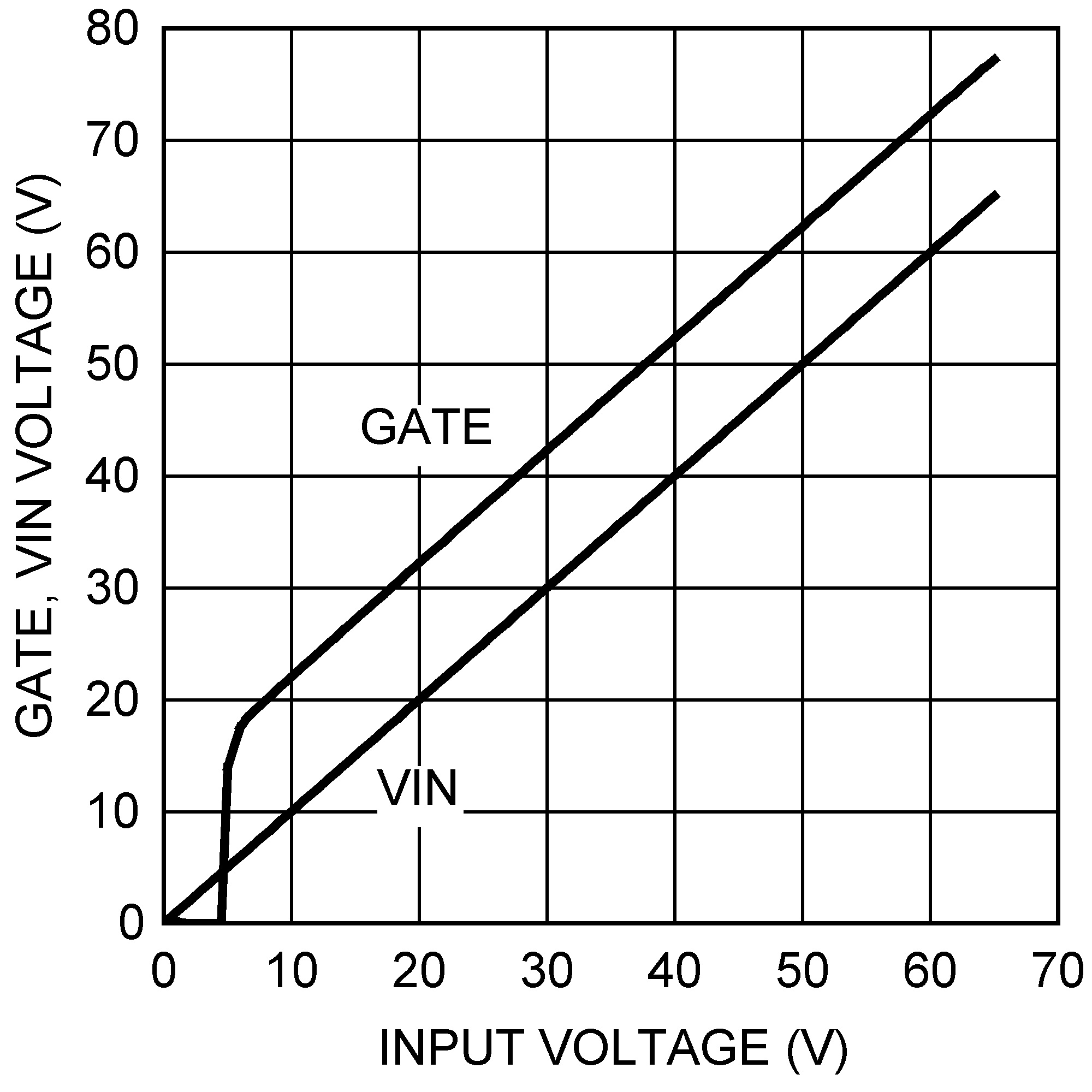 Figure 2. VGATE, VIN Voltage vs Input Voltage
 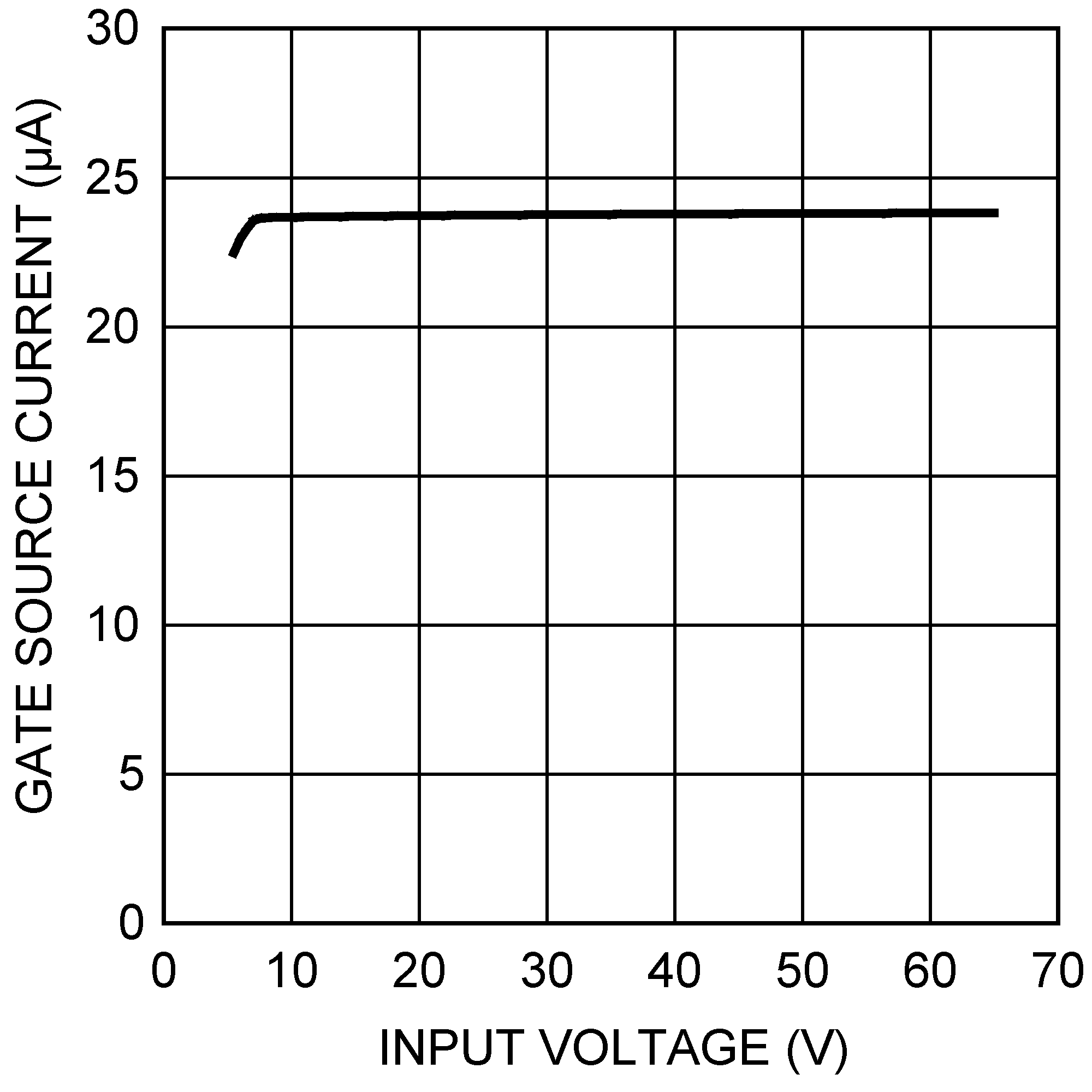 Figure 4. GATE Current (IGATE) vs VIN Voltage
 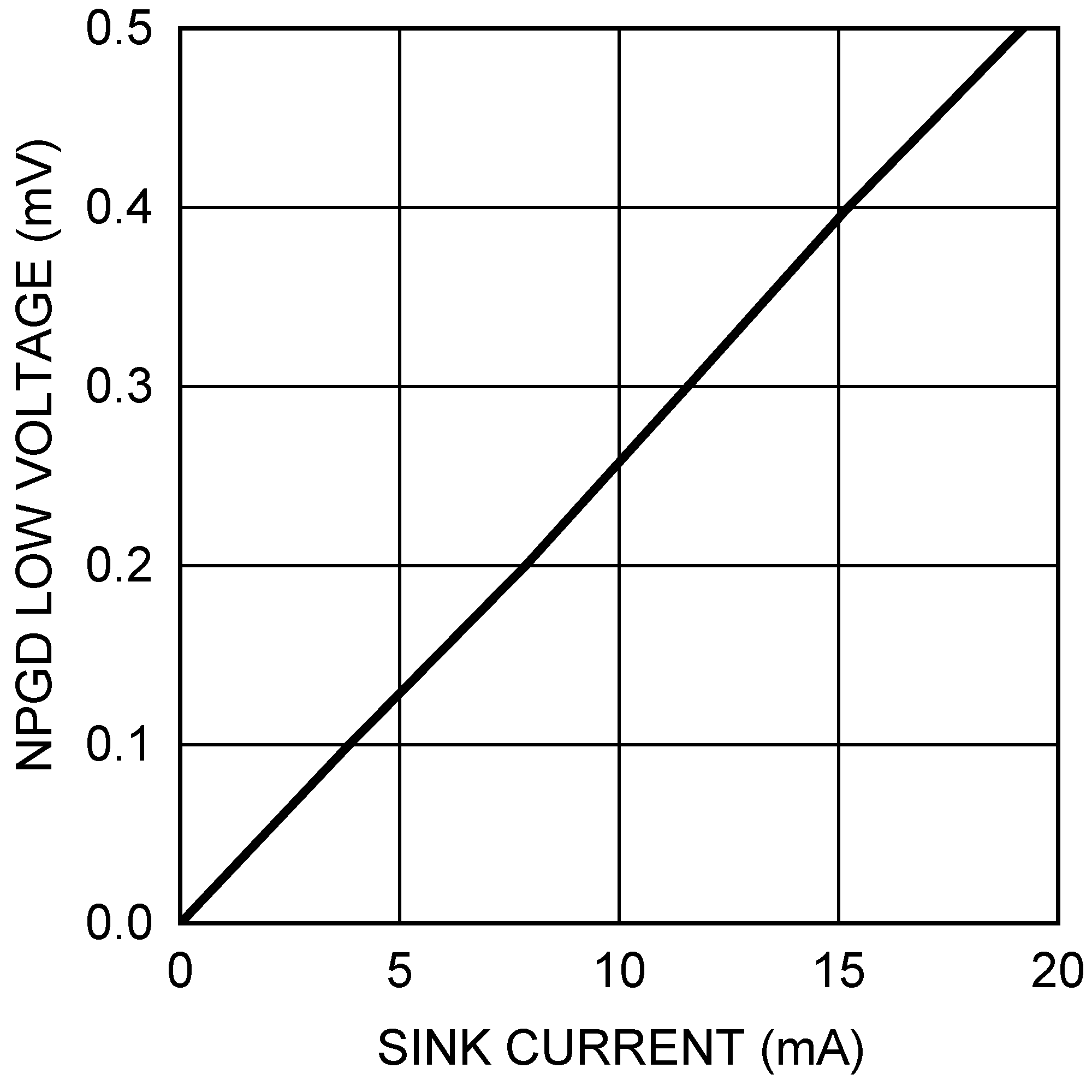 Figure 6. nPGD Low Voltage (PGDVOL vs Sink Current)
 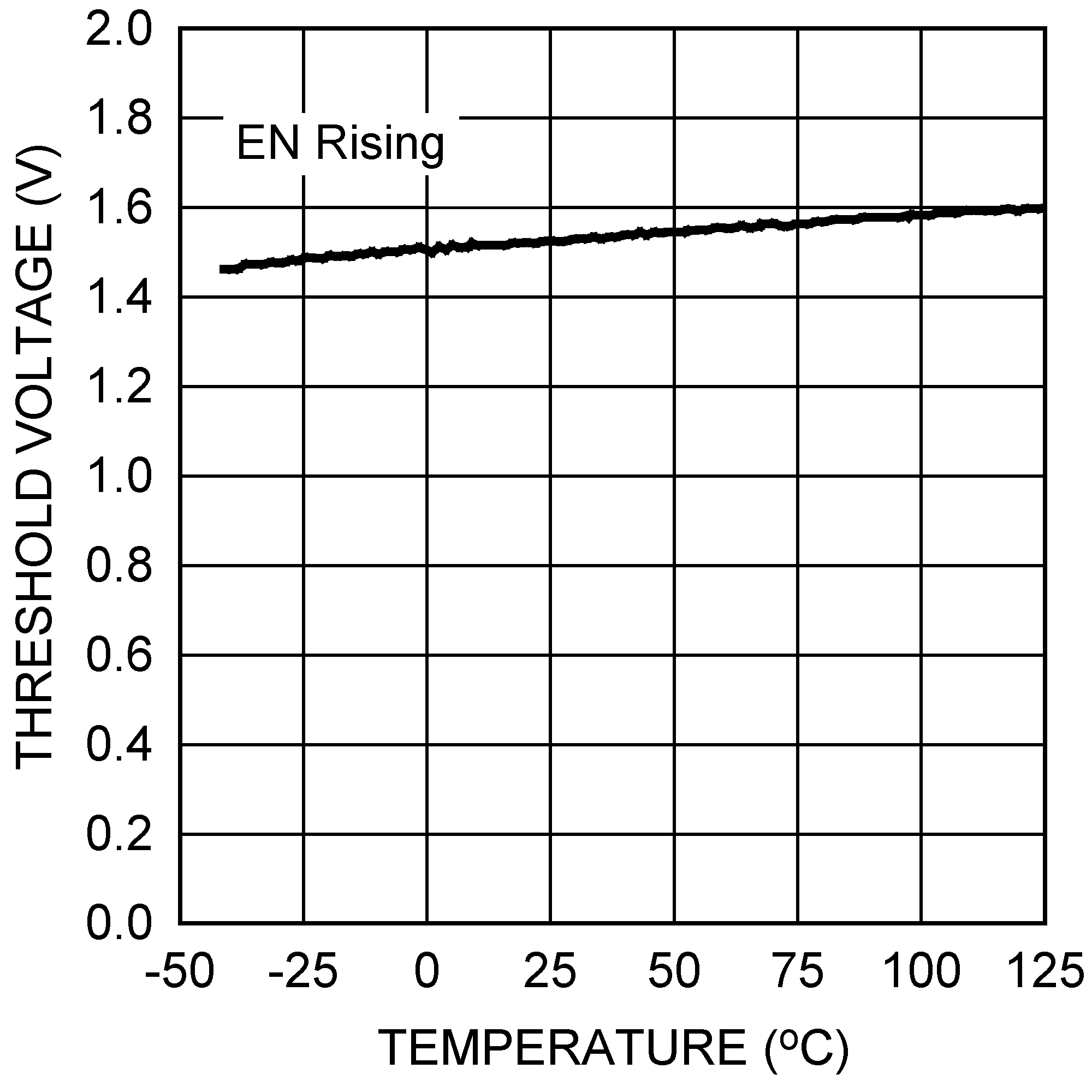 Figure 8. EN Threshold Voltage (ENTH) vs Temperature
 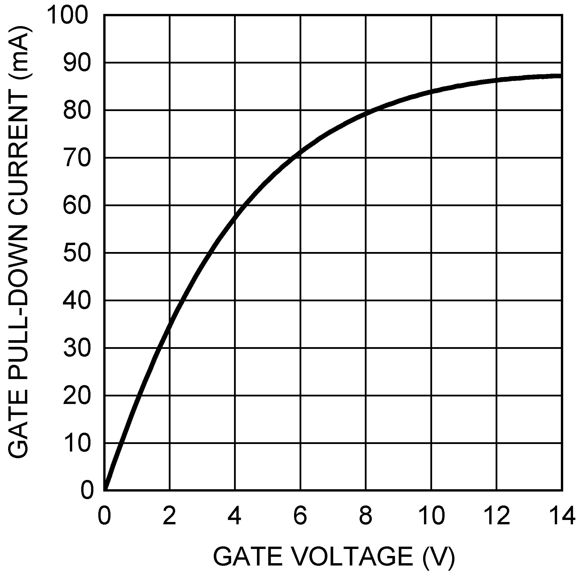 Figure 10. GATE Pull-Down Current Fault (IGATE-FLT)
vs GATE Voltage
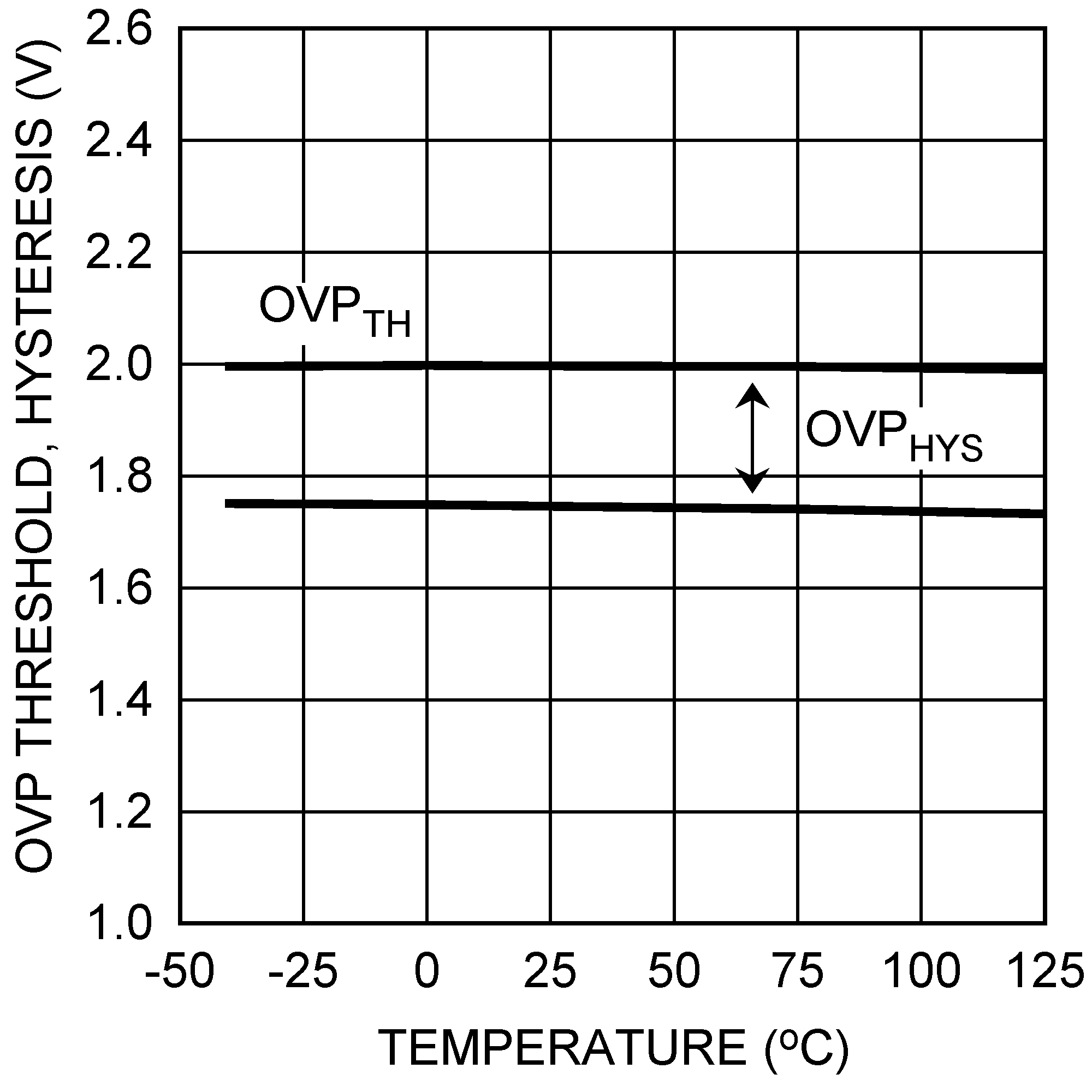 Figure 12. OVP Threshold (OVPTH), Hysteresis (OVPHYS)
vs Temperature
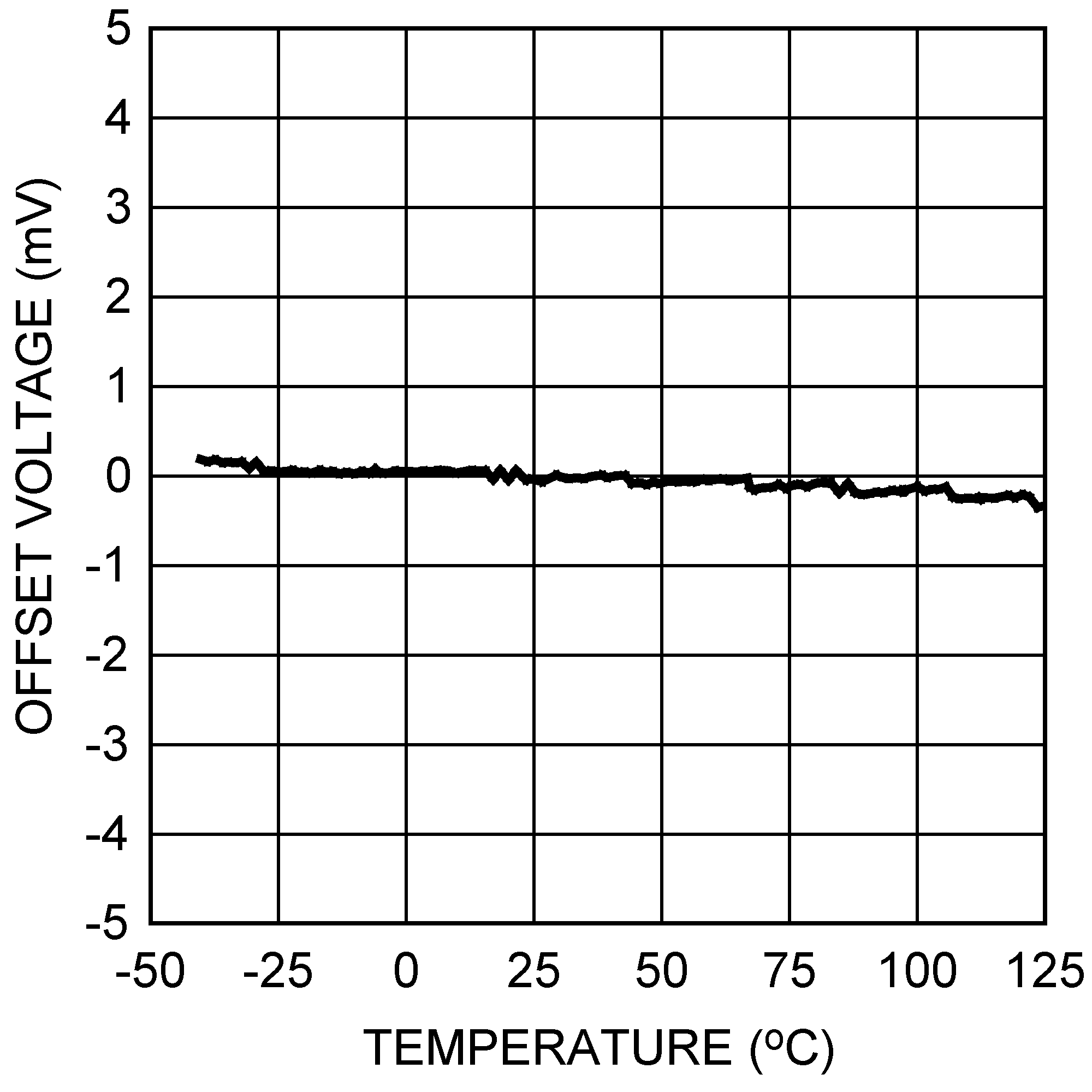 Figure 14. VDS Comparator Offset Voltage (VOFFSET)
vs Temperature
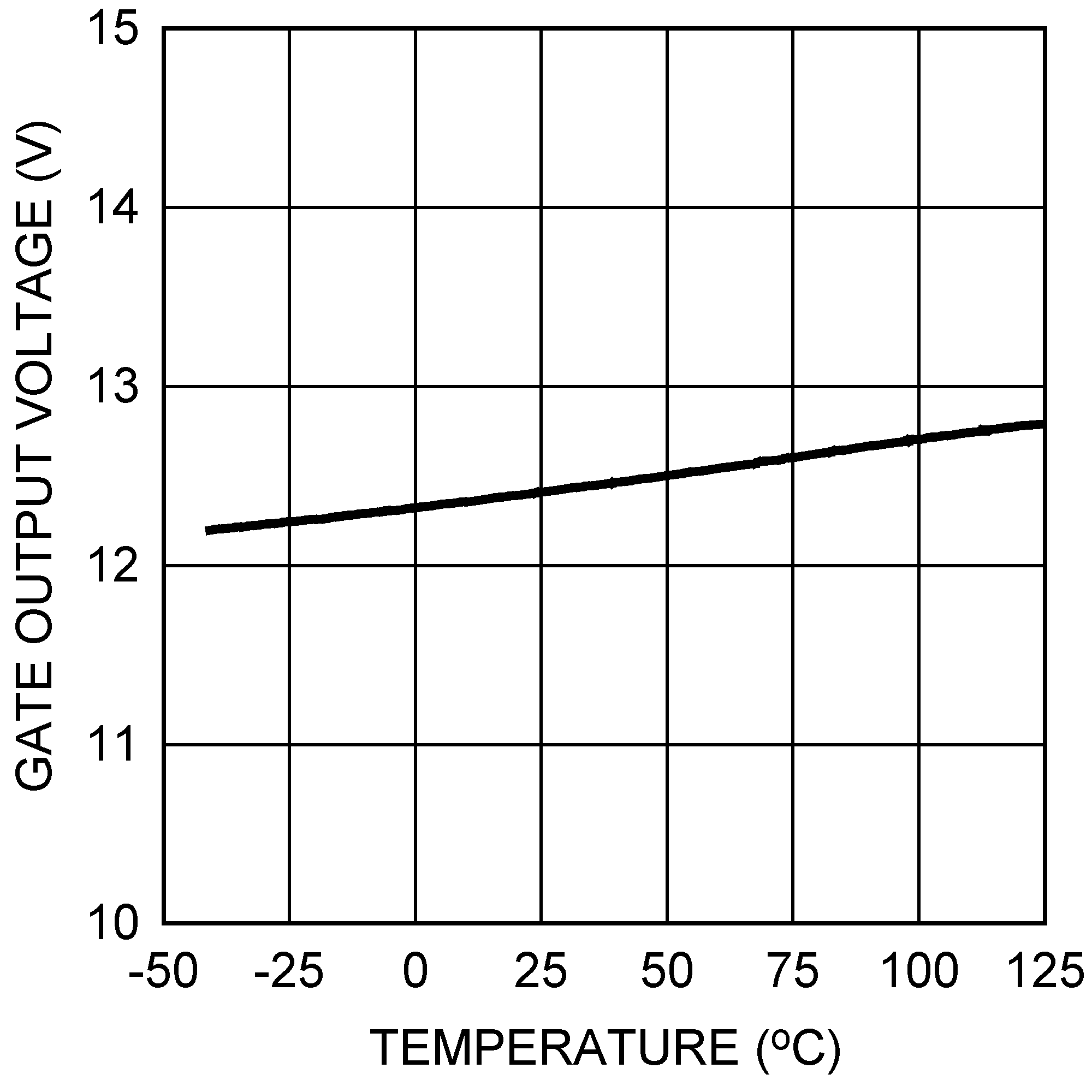 Figure 16. GATE Output Voltage (VGATE) vs Temperature
 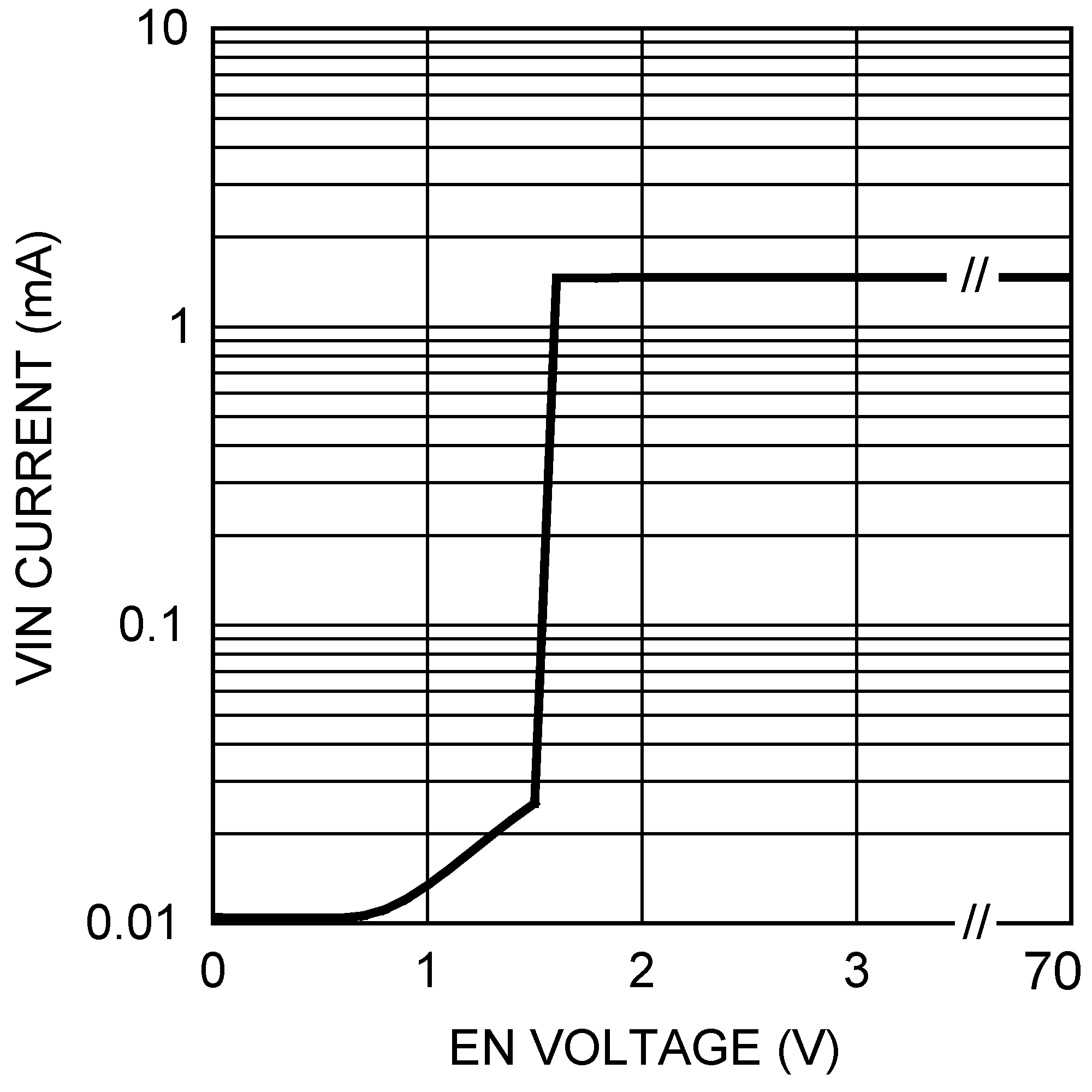 Figure 18. VIN Pin Current (IEN) vs EN Voltage