ZHCSLQ5D October 2007 – August 2020 LM5067
PRODUCTION DATA
- 1 特性
- 2 应用
- 3 说明
- 4 Revision History
- 5 Device Comparison
- 6 Pin Configuration and Functions
- 7 Specifications
- 8 Detailed Description
-
9 Application and Implementation
- 9.1 Application Information
- 9.2
Typical Application
- 9.2.1 Design Requirements
- 9.2.2 Detailed Design Procedure
- 9.2.3 Application Curves
- 10Power Supply Recommendations
- 11Layout
- 12Device and Documentation Support
- 13Mechanical, Packaging, and Orderable Information
8.3.1 Power Up Sequence
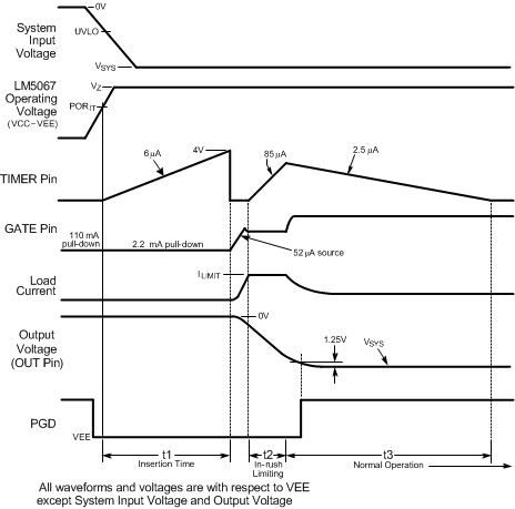
The system voltage range of the LM5067 is –9 V to –80 V, with a transient capability to -100 V. Referring to the Functional Block Diagram, Figure 9-1, and Figure 8-2, as the system voltage (VSYS) initially increases from zero, the external N-channel MOSFET (Q1) is held off by an internal 110 mA pull-down current at the GATE pin. The strong pull-down current at the GATE pin prevents an inadvertent turn-on as the MOSFET’s gate-to-drain (Miller) capacitance is charged. When the operating voltage of the LM5067 (VCC – VEE) reaches the PORIT threshold (7.7V) the insertion timer starts. During the insertion time, the capacitor at the TIMER pin (CT) is charged by a 6 µA current source, and Q1 is held off by a 2.2 mA pull-down current at the GATE pin regardless of the system voltage. The insertion time delay allows ringing and transients at VSYS to settle before Q1 can be enabled. The insertion time ends when the TIMER pin voltage reaches 4 V above VEE, and CT is then quickly discharged by an internal 1.5 mA pull-down current. After the insertion time, the LM5067 control circuitry is enabled when the operating voltage reaches the POREN threshold (8.4 V). As VSYS continues to increase, the LM5067 operating voltage is limited at ≊13 V by an internal zener diode. The remainder of the system voltage is dropped across the input resistor RIN.
The GATE pin switches on Q1 when VSYS exceeds the UVLO threshold (UVLO pin >2.5V above VEE). If VSYS exceeds the UVLO threshold at the end of the insertion time, Q1 is switched on at that time. The GATE pin sources 52 µA to charge Q1’s gate capacitance. The maximum gate-to-source voltage of Q1 is limited by the LM5067’s operating voltage (VZ) to approximately 13 V. During power up, as the voltage at the OUT pin increases in magnitude with respect to Ground, the LM5067 monitors Q1’s drain current and power dissipation. In-rush current limiting and/or power limiting circuits actively control the current delivered to the load. During the in-rush limiting interval (t2 in Figure 8-2) an internal current source charges CT at the TIMER pin. When the load current reduces from the limiting value to a value determined by the load the in-rush limiting interval is complete and CT is discharged. The PGD pin switches high when the voltage at the OUT pin reaches to within 1.25 V of the voltage at the SENSE pin.
If the TIMER pin voltage reaches 4.0V before in-rush current limiting or power limiting ceases (during t2), a fault is declared and Q1 is turned off. See Fault Timer and Restart for a complete description of the fault mode.
 Figure 8-2 Power Up Sequence (Current Limit only)