ZHCSLQ5D October 2007 – August 2020 LM5067
PRODUCTION DATA
- 1 特性
- 2 应用
- 3 说明
- 4 Revision History
- 5 Device Comparison
- 6 Pin Configuration and Functions
- 7 Specifications
- 8 Detailed Description
-
9 Application and Implementation
- 9.1 Application Information
- 9.2
Typical Application
- 9.2.1 Design Requirements
- 9.2.2 Detailed Design Procedure
- 9.2.3 Application Curves
- 10Power Supply Recommendations
- 11Layout
- 12Device and Documentation Support
- 13Mechanical, Packaging, and Orderable Information
9.2.2.9.1 System Considerations During Surge Events
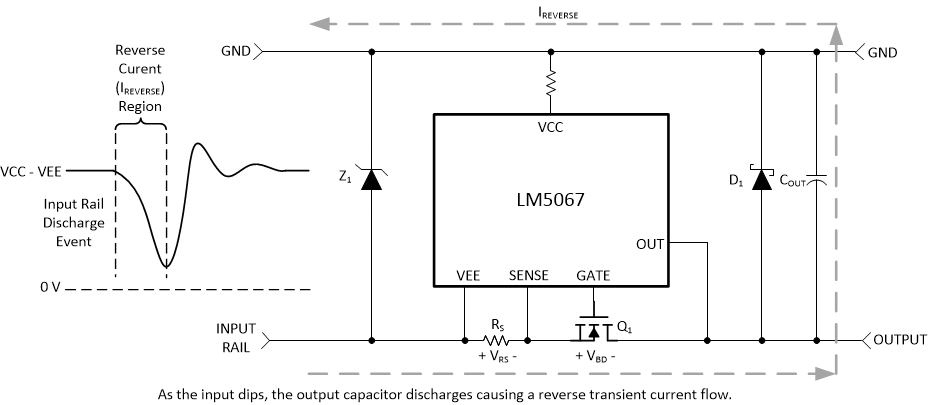
The control MOSFET, Q1, has a body-diode, illustrated in Figure 9-10, where current can freely flow in the reverse direction. The most common cause of a reverse current is a discharge event at the input of the hot-swap circuit when the output capacitance discharges to the input. Normally, reverse current flow presents no issue for hotswap devices during events such as shutdown and minor input power perturbations. However, extreme situations such as high energy lighting surge line disturbances can expose the hot-swap circuit to pulses of ultra fast - high amplitude reverse currents. It is common to observe current amplitudes on the order of 1000 A in these situations. Figure 9-10 illustrates what an extreme input discharge event may look like and how it affects the circuit.
 Figure 9-10 Differential Voltage Across Sense Resistor
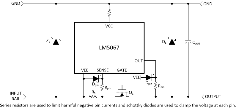
Figure 9-10 shows how the induced reverse current spike causes a differential voltage across the sense resistor, VRS, and the Q1 body-diode, VBD. The transient reverse current, IREVERSE, is approximately equal to IREVERSE = COUT x dVIN/dt because the output capacitor is discharged through the input. Faster discharge rates (dVIN/dt) will induce larger IREVERSE currents. If IREVERSE is extremely high, it can cause a large negative voltage at the SENSE and OUT pins with respect to the VEE pin of the LM5067. If the negative absolute maximum voltage rating is greatly exceeded, harmful currents can flow into the affected pins. Series pin resistors can be implemented to limit the pin current caused by the negative voltage excursion. Schottky diodes may also be implemented to completely clamp the voltage at these pins, Figure 9-11 illustrates this.
 Figure 9-11 Schottky Diodes Used to Clamp Pin Voltage
A typical value of Rpin can be 22 Ω to effectively limit the pin current during extreme negative voltage spikes. If schottky diodes are used, they only need to be applied to SENSE_K, SENSE, and OUT. Each schottky diode return pin should be coupled closely with the VEE plane to provide the most effective clamping. The schottky diode at OUT should be able to withstand at least 100 V. VEE_K needs a series resistor even though it’s not subjected to negative voltage spikes in order to balance the differential current sense voltage signal. Protecting the SENSE_K, SENSE, and OUT pins from negative voltage spikes will facilitate a robust hot-swap circuit and smooth operation during extreme reverse current surge events.