ZHCSJC9G September 2006 – Jaunuary 2020 LM5069
PRODUCTION DATA.
- 1 特性
- 2 应用
- 3 说明
- 4 修订历史记录
- 5 Pin Configuration and Functions
- 6 Specifications
- 7 Detailed Description
-
8 Application and Implementation
- 8.1 Application Information
- 8.2
Typical Application
- 8.2.1
48-V, 10-A Hot Swap Design
- 8.2.1.1 Design Requirements
- 8.2.1.2 Detailed Design Procedure
- 8.2.1.3 Application Curves
- 8.2.1
48-V, 10-A Hot Swap Design
- 9 Power Supply Recommendations
- 10Layout
- 11器件和文档支持
- 12机械、封装和可订购信息
7.4.1 Power Up Sequence
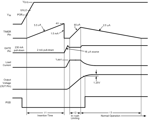
The VIN operating range of the LM5069 is 9 V to 80 V, with a transient capability to 100 V. See Functional Block Diagram and Figure 22, as the voltage at VIN initially increases, the external N-channel MOSFET (Q1) is held off by an internal 230-mA pulldown current at the GATE pin. The strong pulldown current at the GATE pin prevents an inadvertent turnon as the MOSFET’s gate-to-drain (Miller) capacitance is charged. Additionally, the TIMER pin is initially held at ground. When the VIN voltage reaches the PORIT threshold (7.6 V) the insertion time begins. During the insertion time, the capacitor at the TIMER pin (CT) is charged by a 5.5-µA current source, and Q1 is held off by a 2-mA pulldown current at the GATE pin regardless of the VIN voltage. The insertion time delay allows ringing and transients at VIN to settle before Q1 can be enabled. The insertion time ends when the TIMER pin voltage reaches 4 V. CT is then quickly discharged by an internal 1.5-mA pulldown current. After the insertion time, the LM5069 control circuitry is enabled when VIN reaches the POREN threshold (8.4 V). The GATE pin then switches on Q1 when VSYS exceeds the UVLO threshold (UVLO pin >2.5 V). If VSYS is above the UVLO threshold at the end of the insertion time, Q1 switches on at that time. The GATE pin charge pump sources 16 µA to charge Q1’s gate capacitance. The maximum gate-to-source voltage of Q1 is limited by an internal 12-V Zener diode.
As the voltage at the OUT pin increases, the LM5069 monitors the drain current and power dissipation of MOSFET Q1. In-rush current limiting and/or power limiting circuits actively control the current delivered to the load. During the in-rush limiting interval (t2 in Figure 22) an internal 85-µA fault timer current source charges CT. If Q1’s power dissipation and the input current reduce below their respective limiting thresholds before the TIMER pin reaches 4 V, the 85-µA current source is switched off, and CT is discharged by the internal 2.5-µA current sink (t3 in Figure 22). The in-rush limiting interval is complete when the voltage at the OUT pin increases to within 1.25 V of the input voltage (VSYS), and the PGD pin switches high.
If the TIMER pin voltage reaches 4 V before in-rush current limiting or power limiting ceases (during t2), a fault is declared and Q1 is turned off. See Fault Timer and Restart for a complete description of the fault mode.
 Figure 22. Power-Up Sequence (Current Limit Only)