ZHCSJC9G September 2006 – Jaunuary 2020 LM5069
PRODUCTION DATA.
- 1 特性
- 2 应用
- 3 说明
- 4 修订历史记录
- 5 Pin Configuration and Functions
- 6 Specifications
- 7 Detailed Description
-
8 Application and Implementation
- 8.1 Application Information
- 8.2
Typical Application
- 8.2.1
48-V, 10-A Hot Swap Design
- 8.2.1.1 Design Requirements
- 8.2.1.2 Detailed Design Procedure
- 8.2.1.3 Application Curves
- 8.2.1
48-V, 10-A Hot Swap Design
- 9 Power Supply Recommendations
- 10Layout
- 11器件和文档支持
- 12机械、封装和可订购信息
8.2.1.1 Design Requirements
Table 1 summarizes the design parameters that must be known before designing a hot swap circuit. When charging the output capacitor through the hot swap MOSFET, the FET’s total energy dissipation equals the total energy stored in the output capacitor (½CV2). Thus, both the input voltage and output capacitance determine the stress experienced by the MOSFET. The maximum load current drives the current limit and sense resistor selection. In addition, the maximum load current, maximum ambient temperature, and the thermal properties of the PCB (RθCA) drive the selection of the MOSFET RDSON and the number of MOSFETs used. RθCA is a strong function of the layout and the amount of copper that is connected to the drain of the MOSFET. Note that the drain is not electrically connected to the ground plane and thus the ground plane cannot be used to help with heat dissipation. For this design example RθCA = 30°C/W is used, which is similar to the LM5069 EVM. It’s a good practice to measure the RθCA of a given design after the physical PCBs are available.
Finally, it’s important to understand what test conditions the hot swap must pass. In general, a hot swap is designed to pass both a Hot-Short and a Start into a Short. Also, TI recommends keeping the load OFF until the hot swap is fully powered up. Starting the load early causes unnecessary stress on the MOSFET and could lead to MOSFET failures or a failure to start-up.
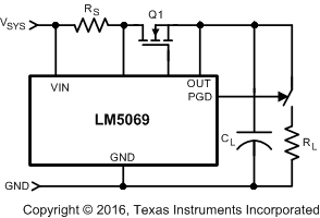
 Figure 28. No Load Current During Turnon
 Table 1. Design Parameters
| PARAMETER | VALUE |
|---|---|
| Input voltage range | 18 to 30 V |
| Maximum load current | 10 A |
| Lower UVLO threshold | 17 V |
| Upper UVLO threshold | 18 V |
| Lower OVLO threshold | 30 V |
| Upper OVLO threshold | 31 V |
| Maximum output capacitance of the hot swap | 330 µF |
| Maximum ambient temperature | 55°C |
| MOSFET RθCA (function of layout) | 30°C/W |
| Pass Hot-short on output? | Yes |
| Pass a Start into short? | Yes |
| Is the load off until PG asserted? | Yes |
| Can a hot board be plugged back in? | No |