ZHCSJC9G September 2006 – Jaunuary 2020 LM5069
PRODUCTION DATA.
- 1 特性
- 2 应用
- 3 说明
- 4 修订历史记录
- 5 Pin Configuration and Functions
- 6 Specifications
- 7 Detailed Description
-
8 Application and Implementation
- 8.1 Application Information
- 8.2
Typical Application
- 8.2.1
48-V, 10-A Hot Swap Design
- 8.2.1.1 Design Requirements
- 8.2.1.2 Detailed Design Procedure
- 8.2.1.3 Application Curves
- 8.2.1
48-V, 10-A Hot Swap Design
- 9 Power Supply Recommendations
- 10Layout
- 11器件和文档支持
- 12机械、封装和可订购信息
10.1.1 PC Board Guidelines
The following guidelines must be followed when designing the PC board for the LM5069:
- Place the LM5069 close to the board’s input connector to minimize trace inductance from the connector to the FET.
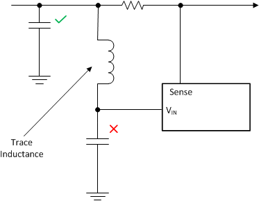
- Note that special care must be taken when placing the bypass capacitor for the VIN pin. During hot shorts, there is a very large dV/dt on input voltage after the MOSFET turns off. If the bypass capacitor is placed right next to the pin and the trace from Rsns to the pin is long, an LC filter is formed. As a result, a large differential voltage can develop between VIN and SENSE. To avoid this, place the bypass capacitor close to Rsns instead of the VIN pin.
- The sense resistor (RS) must be close to the LM5069, and connected to it using the Kelvin techniques shown in Figure 46.
- The high current path from the board’s input to the load (via Q1), and the return path, must be parallel and close to each other to minimize loop inductance.
- The ground connection for the various components around the LM5069 must be connected directly to each other, and to the LM5069’s GND pin, and then connected to the system ground at one point. Do not connect the various component grounds to each other through the high current ground line.
- Provide adequate heat sinking for the series pass device (Q1) to help reduce stresses during turnon and turnoff.
- The board’s edge connector can be designed to shut off the LM5069 as the board is removed, before the supply voltage is disconnected from the LM5069. In Figure 45 the voltage at the UVLO pin goes to ground before VSYS is removed from the LM5069 due to the shorter edge connector pin. When the board is inserted into the edge connector, the system voltage is applied to the LM5069’s VIN pin before the UVLO voltage is taken high.
 Figure 43. Layout Trace Inductance