SNVS565I November 2008 – August 2015 LM5085 , LM5085-Q1
PRODUCTION DATA.
- 1 Features
- 2 Applications
- 3 Description
- 4 Revision History
- 5 Pin Configuration and Functions
- 6 Specifications
- 7 Detailed Description
- 8 Application and Implementation
- 9 Power Supply Recommendations
- 10Layout
- 11Device and Documentation Support
- 12Mechanical, Packaging, and Orderable Information
封装选项
请参考 PDF 数据表获取器件具体的封装图。
机械数据 (封装 | 引脚)
- NGQ|8
- DGK|8
- DGN|8
散热焊盘机械数据 (封装 | 引脚)
- DGN|8
订购信息
7 Detailed Description
7.1 Overview
The LM5085 is a PFET buck (step-down) DC-DC controller using the constant on-time (COT) control principle. The input operating voltage range of the LM5085 is 4.5V to 75V. The use of a PFET in a buck regulator greatly simplifies the gate drive requirements and allows for 100% duty cycle operation to extend the regulation range when operating at low input voltage. However, PFET transistors typically have higher on-resistance and gate charge when compared to similarly rated NFET transistors. Consideration of available PFETs, input voltage range, gate drive capability of the LM5085, and thermal resistances indicate an upper limit of 10A for the load current for LM5085 applications. Constant on-time control is implemented using an on-time one-shot that is triggered by the feedback signal. During the off-time, when the PFET (Q1) is off, the load current is supplied by the inductor and the output capacitor. As the output voltage falls, the voltage at the feedback comparator input (FB) falls below the regulation threshold. When this occurs Q1 is turned on for the one-shot period which is determined by the input voltage (VIN) and the RT resistor. During the on-time the increasing inductor current increases the voltage at FB above the feedback comparator threshold. For a buck regulator the basic relationship between the on-time, off-time, input voltage and output voltage is:

where Fs is the switching frequency. Equation 1 is valid only in continuous conduction mode (inductor current does not reach zero). Since the LM5085 controls the on-time inversely proportional to VIN, the switching frequency remains relatively constant as VIN is varied. If the input voltage falls to a level that is equal to or less than the regulated output voltage Q1 is held on continuously (100% duty cycle) and VOUT is approximately equal to VIN.
The COT control scheme, with the feedback signal applied to a comparator rather than an error amplifier, requires no loop compensation, resulting in very fast load transient response.
The LM5085 is available in both an 8-pin HVSSOP package and an 8-pin WSON package with an exposed pad to aid in heat dissipation. An 8-pin VSSOP package without an exposed pad is also available.
7.2 Functional Block Diagram

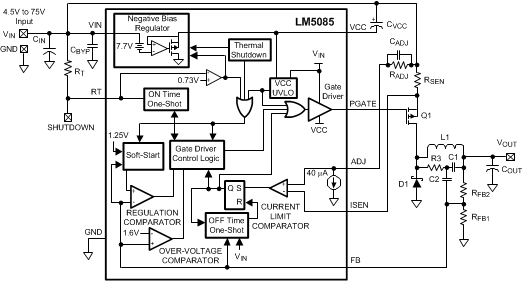
Minimum output ripple configuration shown.
7.3 Feature Description
7.3.1 Regulation Control Circuit
The LM5085 buck DC-DC controller employs a control scheme based on a comparator and a one-shot on-timer, with the output voltage feedback compared to an internal reference voltage (1.25V). When the FB pin voltage falls below the feedback reference, Q1 is switched on for a time period determined by the input voltage and a programming resistor (RT). Following the on-time Q1 remains off until the FB voltage falls below the reference. Q1 is then switched on for another on-time period. The output voltage is set by the feedback resistors (RFB1, RFB2 in the Block Diagram). The regulated output voltage is calculated as follows:
The feedback voltage supplied to the FB pin is applied to a comparator rather than a linear amplifier. For proper operation sufficient ripple amplitude is necessary at the FB pin to switch the comparator at regular intervals with minimum delay and noise susceptibility. This ripple is normally obtained from the output voltage ripple attenuated through the feedback resistors. The output voltage ripple is a result of the inductor’s ripple current passing through the output capacitor’s ESR, or through a resistor in series with the output capacitor. Multiple methods are available to ensure sufficient ripple is supplied to the FB pin, and three different configurations are discussed in the Typical Application section.
When in regulation, the LM5085 operates in continuous conduction mode at medium to heavy load currents and discontinuous conduction mode at light load currents. In continuous conduction mode the inductor’s current is always greater than zero, and the operating frequency remains relatively constant with load and line variations. The minimum load current for continuous conduction mode is one-half the inductor’s ripple current amplitude. In discontinuous conduction mode, where the inductor’s current reaches zero during the off-time, the operating frequency is lower than in continuous conduction mode and varies with load current. Conversion efficiency is maintained at light loads since the switching losses are reduced with the reduction in load and frequency.
If the voltage at the FB pin exceeds 1.6V due to a transient overshoot or excessive ripple at VOUT the internal over-voltage comparator immediately switches off Q1. The next on-time period starts when the voltage at FB falls below the feedback reference voltage.
7.3.2 On-Time Timer
The on-time of the PFET gate drive output (PGATE pin) is determined by the resistor (RT) and the input voltage (VIN), and is calculated from:

where RT is in kΩ.
The minimum on-time, which occurs at maximum VIN, should not be set less than 150ns (see Current Limiting section). The buck regulator effective on-time, measured at the SW node (junction of Q1, L1, and D1) is typically longer than that calculated in Equation 3 due to the asymmetric delay of the PFET. The on-time difference caused by the PFET switching delay can be estimated as the difference of the turn-off and turn-on delays listed in the PFET data sheet. Measuring the difference between the on-time at the PGATE pin versus the SW node in the actual application circuit is also recommended.
In continuous conduction mode, the inverse relationship of tON with VIN results in a nearly constant switching frequency as VIN is varied. The operating frequency can be calculated from:

where RT is in kΩ, and tD is equal to 50ns plus the PFET’s delay difference. To set a specific continuous conduction mode switching frequency (FS), the RT resistor is determined from the following:

where RT is in kΩ. A simplified version of Equation 5 at VIN = 12V, and tD = 100ns, is:

For VIN = 48V and tD = 100ns, the simplified equation is:

7.3.3 Shutdown
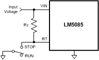
The LM5085 can be shutdown by grounding the RT pin (see Figure 22). In this mode the PFET is held off, and the VCC regulator is disabled. The internal operating current is reduced to the value shown in the graph “Shutdown current vs. VIN”. The shutdown threshold at the RT pin is ≊0.73V, with ≊50mV of hysteresis. Releasing the pin enables normal operation. The RT pin must not be forced high during normal operation.
 Figure 22. Shutdown Implementation
7.3.4 Current Limiting
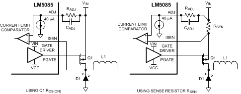
The LM5085 current limiting operates by sensing the voltage across either the RDS(ON) of Q1, or a sense resistor, during the on-time and comparing it to the voltage across the resistor RADJ (see Figure 23). The current limit function is much more accurate and stable over temperature when a sense resistor is used. The RDS(ON) of a MOSFET has a wide process variation and a large temperature coefficient.
If the voltage across RDS(ON) of Q1, or the sense resistor, is greater than the voltage across RADJ, the current limit comparator switches to turn off Q1. Current sensing is disabled for a blanking time of ≊100ns at the beginning of the on-time to prevent false triggering of the current limit comparator due to leading edge current spikes. Because of the blanking time and the turn-on and turn-off delays created by the PFET, the on-time at the PGATE pin should not be set less than 150ns. An on-time shorter than that may prevent the current limit detection circuit from properly detecting an over-current condition. The duration of the subsequent forced off-time is a function of the input voltage and the voltage at the FB pin, as shown in the graph “Off-time vs. VIN and VFB”. The longer-than-normal forced off-time allows the inductor current to decrease to a low level before the next on-time. This cycle-by-cycle monitoring, followed by a forced off-time, provides effective protection from output load faults over a wide range of operating conditions.
The voltage across the RADJ resistor is set by an internal 40µA current sink at the ADJ pin. When using Q1’s RDS(ON) for sensing, the current at which the current limit comparator switches is calculated from:
When using a sense resistor (RSEN) the threshold of the current limit comparator is calculated from:
When using Equation 8 or Equation 9, the tolerances for the ADJ pin current sink and the offset of the current limit comparator should be included to ensure the resulting minimum current limit is not less than the required maximum switch current. Simultaneously increasing the values of RADJ and RSEN decreases the effects of the current limit comparator offset, but at the expense of higher power dissipation. When using a sense resistor, the RSEN resistor value should be chosen within the practical limitations of power dissipation and physical size. For example, for a 10A current limit, setting RSEN = 0.005Ω results in a power dissipation as high as 0.5W. Current sense connections to the RSEN resistor, or to Q1, must be Kelvin connections to ensure accuracy.
The CADJ capacitor filters noise from the ADJ pin, and helps prevent unintended switching of the current limit comparator due to input voltage transients. The recommended value for CADJ is 1000pF.
7.3.5 Current Limit Off-Time
When the current through Q1 exceeds the current limit threshold, the LM5085 forces an off-time longer than the normal off-time defined by Equation 1. See the graph “Off-Time vs. VIN and VFB”, or calculate the current limit off-time from the following equation:

where VIN is the input voltage, and VFB is the voltage at the FB pin at the time current limit was detected. This feature is necessary to allow the inductor current to decrease sufficiently to offset the current increase which occurred during the on-time. During the on-time, the inductor current increases an amount equal to:

During the off-time the inductor current decreases due to the reverse voltage applied across the inductor by the output voltage, the freewheeling diode’s forward voltage (VFD), and the voltage drop due to the inductor’s series resistance (VESR). The current decrease is equal to:

The on-time in Equation 11 is shorter than the normal on-time since the PFET is shut off when the current limit threshold is crossed. If the off-time is not long enough, such that the current decrease (Equation 12) is less than the current increase (Equation 11), the current levels are higher at the start of the next on-time. This results in a further decrease in on-time, since the current limit threshold is crossed sooner. A balance is reached when the current changes in Equation 11 and Equation 12 are equal. The worst case situation is that of a direct short circuit at the output terminals, where VOUT = 0V, as that results in the largest current increase during the on-time, and the smallest decrease during the off-time. The sum of the diode’s forward voltage and the inductor’s ESR voltage must be sufficient to ensure current runaway does not occur. Using Equation 11 and Equation 12, this requirement can be stated as:

For tON in Equation 13, use the minimum on-time at the SW node. To determine this time period add the “Minimum On-Time in Current Limit” specified in the Electrical Characteristics (tON-4) to the difference of the turn-off and turn-on delays of the PFET. For tOFF use the value in the graph “Off-Time vs. VIN and VFB”, or use Equation 10, where VFB is equal to zero volts. When using the minimum or maximum limits of those specifications to determine worst case situations, the tolerance of the minimum on-time (tON-4) and the current limit off-times (tOFF(CL1) through tOFF(CL4)) track each other over the process and temperature variations. A device which has an on-time at the high end of the range will have an off-time that is at the high end of its range.
 Figure 23. Current Limit Sensing
7.3.6 VCC Regulator
The VCC regulator provides a regulated voltage between the VIN and the VCC pins to provide the bias and gate current for the PFET gate driver. The 0.47µF capacitor at the VCC pin must be a low ESR capacitor, preferably ceramic as it provides the high surge current for the PFET’s gate at each turn-on. The capacitor must be located as close as possible to the VIN and VCC pins to minimize inductance in the PC board traces.
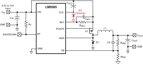
Referring to Figure 4 “VCC vs. VIN”, the voltage across the VCC regulator (VIN – VCC) is equal to VIN until VIN reaches approximately 8.5V. At higher values of VIN, the voltage at the VCC pin is regulated at approximately 7.7V below VIN. If VIN drops below about 8V due to voltage transients, the VCC pin can be pulled down below GND. To prevent the negative VCC voltage from disturbing the internal circuit and causing abnormal operation, Figure 24 shows the required placement of this Schottky diode between the VCC pin and GND pin. The Schottky diode should be placed as close as possible to the VCC pin. The VCC regulator has a maximum current capability of at least 20mA. The regulator is disabled when the LM5085 is shutdown using the RT pin, or when the thermal shutdown is activated.
 Figure 24. Schottky Diode at VCC Pin During VIN Negative Transients (VIN < 8 V)
7.3.7 PGATE Driver Output
The PGATE pin output swings between VIN (Q1 off) and the VCC pin voltage (Q1 on). The rise and fall times depend on the PFET gate capacitance and the source and sink currents provided by the internal gate driver. See the Electrical Characteristics for the current capability of the driver.
7.3.8 P-Channel MOSFET Selection
The PFET must be rated for the maximum input voltage, with some margin above that to allow for transients and ringing which can occur on the supply line and the switching node. The gate-to-source voltage (VGS) normally provided to the PFET is 7.7V for VIN greater than 8.5V. However, if the circuit is to be operated at lower values of VIN, the selected PFET must be able to fully turn-on with a VGS voltage equal to VIN. The minimum input operating voltage for the LM5085 is 4.5V.
Similar to NFETs, the case or exposed thermal pad for a PFET is electrically connected to the drain terminal. When designing a PFET buck regulator the drain terminal is connected to the switching node. This situation requires a trade-off between thermal and EMI performance since increasing the PC board area of the switching node to aid the PFET power dissipation also increases radiated noise, possibly disrupting the circuit operation. Typically the switching node area is kept to a reasonable minimum and the PFET peak current is derated to stay within the recommended temperature rating of the PFET. The RDS(ON) of the PFET determines a portion of the power dissipation in the PFET. However, PFETs with very low RDS(ON) usually have large values of gate charge. A PFET with a higher gate charge has a corresponding slower switching speed, leading to higher switching losses and affecting the PFET power dissipation.
If the PFET RDS(ON) is used for current limit detection, note that it typically has a positive temperature coefficient. At 100°C the RDS(ON) may be as much as 50% higher than the value at 25°C which could result in incorrect current limiting if not accounted for when determining the value of the RADJ resistor. The PFET Total Gate Charge determines most of the power dissipation in the LM5085 due to the repetitive charge and discharge of the PFET’s gate capacitance by the gate driver (powered from the VCC regulator). The LM5085’s internal power dissipation can be calculated from the following:
where QG is the PFET's Total Gate Charge obtained from its datasheet, FS is the switching frequency, and IIN is the LM5085's operating current obtained from the graph "Input Operating Current vs. VIN". Using the Thermal Resistance specifications in the Electrical Characteristics table, the approximate junction temperature can be determined. If the calculated junction temperature is near the maximum operating temperature of 125°C, either the switching frequency must be reduced, or a PFET with a smaller Total Gate Charge must be used.
7.3.9 Soft-Start
The internal soft-start feature of the LM5085 allows the regulator to gradually reach a steady state operating point at power up, thereby reducing startup stresses and current surges. Upon turn-on, when Vcc reaches its under-voltage lockout threshold, the internal soft-start circuit ramps the feedback reference voltage from 0V to 1.25V, causing VOUT to ramp up in a proportional manner. The soft-start ramp time is typically 2.5ms.
In addition to controlling the initial power up cycle, the soft-start circuit also activates when the LM5085 is enabled by releasing the RT pin, and when the circuit is shutdown and restarted by the internal Thermal Shutdown circuit.
If the voltage at FB is below the regulation threshold value due to an over-current condition or a short circuit at VOUT, the internal reference voltage provided by the soft-start circuit to the regulation comparator is reduced along with FB. When the over-current or short circuit condition is removed, VOUT returns to the regulated value at a rate determined by the soft-start ramp. This feature helps prevent the output voltage from overshooting following an overload event.
7.3.10 Thermal Shutdown
The LM5085 should be operated such that the junction temperature does not exceed 125°C. If the junction temperature increases above that, an internal Thermal Shutdown circuit activates at 170°C (typical) to disable the VCC regulator and the gate driver, and discharge the soft-start capacitor. This feature helps prevent catastrophic failures from accidental device overheating. When the junction temperature falls below 150°C (typical hysteresis = 20°C), the gate driver is enabled, the soft-start circuit is released, and normal operation resumes.
7.4 Device Functional Modes
7.4.1 Standby Mode with VIN <4.5 V
The LM5085 is intended to operate with input voltages above 4.5 V. The minimum operating input voltage is determined by the VCC undervoltage lockout threshold of 3.8 V (typ). If VIN is too low to support a VCC voltage greater than the VCC UVLO threshold, the controller switches to the standby mode with the PFET buck switch in the off state.
7.4.2 RT Shutdown Mode
The LM5085 is in shutdown mode when the RT pin is pulled below 0.73 V (typ). In this mode, the PFET gate driver is held off and the VCC regulator is disabled.